

Introduction to FPGA Design
Field-programmable gate arrays, or FPGAs, are a rapidly expanding field that is grabbing the interest of major international companies and investors.
It is expected to keep expanding in the years to come.
FPGA technology is a well-liked choice in numerous industries, such as consumer electronics, telecommunications, automotive, and aerospace.
To application-specific integrated circuits (ASICs), field programmable gate array technology is undergoing a noteworthy trend of constant improvement.
Due to aspects including reduced turnaround time, cost-effectiveness, and decreased power consumption.
Because of their inherent flexibility, FPGAs are becoming more and more popular as a means of reconfiguring circuits after implementation.
According to Polaris Market Research, Field Programmable Gate Array Market size was valued at USD 11.74 billion in 2023. The market is anticipated to grow from USD 12.94 billion in 2024 to USD 28.81 billion by 2032, exhibiting a CAGR of 10.5% during the forecast period.

The increasing number of data centers and facilities devoted to high-performance computing (HPC), the widespread integration of artificial intelligence (AI), and Internet of Things (IoT) technologies.
Across a wide range of applications and the fact that Field-Programmable Gate Arrays (FPGAs) are more efficient than application-specific integrated circuits (ASICs) are the factors propelling the growth of the FPGA market.
All the information you want to understand about FPGA design will be covered in this comprehensive guide, including FPGA architecture, parts, applications, development process, verification, benefits and drawbacks, and more.
Understanding FPGA Basics
Integrated circuits that can be programmed even after they are manufactured are called Field Programmable Gate Arrays, or FPGAs.
They offer flexibility, parallel processing, and customizability for various applications like aerospace, automotive, and telecommunications.
FPGA provides you the ability to customize them to meet your unique demands by enabling parallel processing.
They are a great option for intricate, dynamic projects since you can quickly reprogram and upgrade them using languages like Verilog and VHDL.
What is an FPGA?
A field-programmable gate array (FPGA) is a type of configurable integrated circuit that can be repeatedly programmed after manufacturing.
FPGAs offer a unique approach to implementing digital circuits by providing programmable hardware blocks and interconnects that can be configured to perform a wide range of tasks.

History of FPGA

Here is a brief timeline of some of the inventions that have led to FPGA technology.
1970 — PROM
One of the earliest forms of programmable memory was PROM (programmable read-only memory).
Read-only memory, or ROM, was used in the past to store data throughout manufacture.
Since PROM couldn’t be reprogrammed, there was still room for improvement even if it was a significant advancement in programmable technology.
1971 — EPROM
Erasable programmable read-only memory, or EPROM, was the next development in programmable memory, with the ability to be erased.
An EPROM has to be directly exposed to UV light to be erased.
Nevertheless, since you would need to remove the EPROM from the circuit to erase it, this method of erasing is not the most practical.
Programmable read-only memory (PROM) and programmable logic devices (PLDs) gave rise to the FPGA business.
It was possible to program PROMs and PLDs in batches in a factory or on-site (field-programmable).
The Naval Surface Warfare Center provided financing for an experiment proposed by Steve Casselman that resulted in the creation of the FPGA concept in the late 1980s.
He proposed to build a computer system with more than 600,000 reprogrammable gates.
A company by the name of Altera invented the first reprogrammable logic device in 1984.
The EP300 model had a window that let ultraviolet light reach EPROM cells, allowing for their erasure.
The design configuration was stored in the cells, so it could be altered as needed.
LuVerne R. Peterson and David W. Page’s 1985 patents for logic blocks, gates, and programmable logic arrays broadened the basis of FPGA.
FPGA had taken the industry by storm by the mid-1990s when it began to explode.
Even though networking and telecommunications benefited most at the time, FPGA was now used in consumer, industrial, and automotive applications for many kinds of electronic devices.
FPGAs are currently found in all computable devices since they maximize the amount of gates employed and are faster in some applications.
These devices can be found in a wide range of industries and applications, including the following:
- Aerospace, Outer Space, and Defense
- Audio, Automotive, and Broadcast
- Consumer Electronics, Data Centers, and High-Performance Computing
- Instruments of Science, Industrial, and Medical
- Security Applications, Wired & Wireless Communications, and More
FPGA has impacted a wide range of industries, and this list is expanding as more and more elements of people’s lives are being impacted by electronic gadgets.
Related Post: Introduction to FPGA – History, Architecture, Application & Market Growth
FPGA Architecture
Configurable logic blocks, or CLBs, are the building blocks of a basic FPGA design.
They are made up of thousands of core components that are connected by a programmable fabric system that routes signals between CLBs.
Interfacing the FPGA with external devices is obstructed by input/output (I/O).
The two-dimensional arrays of logic blocks in the basic FPGA architecture allow the user to configure how the logic blocks are connected.
The functions of an FPGA architecture module are discussed below,

FPGAs can be classified into three groups based on their internal block arrangement:
Symmetrical arrays
The logic components, also known as CLBs, are arranged in a matrix’s rows and columns with connections established between them.
This symmetrical matrix is surrounded by I/O blocks that link it to the external environment.
Each CLB consists of an n-input Lookup table and two programmable flip-flops.
I/O blocks also regulate functions like output transition speed and tristate control. A routing path is created using interconnects.
Direct interconnects between adjacent logic elements have a shorter delay than general-purpose interconnects.
Row-based architecture
A row-based design consists of alternating rows of logic modules and programmable connecting tracks.
The rows’ outer edges are where the input-output blocks are situated. One row can be connected to adjacent rows via vertical interconnects.
There are numerous ways to join logic modules. All of the components that make up combinatorial modules are combinational.
Sequential modules come with flip-flop and combinational functionalities.
This sequential module can be used to build complex combinatorial-sequential functions.
The smaller sections of the routing rails are connected with anti-fuse parts.
Hierarchical PLDs
This architecture consists of only logic blocks and interconnects at the top level, arranged hierarchically.
Every logic block consists of several logic modules. There are sequential and combinatorial functional aspects in every logic module.
All these working components are under the control of the programmed memory.
Logic blocks can communicate with one another through programmable interconnect arrays.
Input-output used blocks around this system of logic blocks and interconnects.
Components of an FPGA
In addition to more general-purpose customizable logic, modern FPGAs often have components designed for specific purposes.
Power-efficient and highly efficient designs have been made possible by the marriage of flexible logic with specific functionality components.
This brings us to a closer look at the construction of an FPGA. Three fundamental parts typically make up an FPGA. like this:
Configurable Logic Blocks (CLBs)
These are the fundamental components that make up an FPGA; they include flip-flops, look-up tables (LUTs), and occasionally specialized arithmetic units.
Different combinational and sequential logic operations can be set up for CLBs.
The logic blocks of an FPGA can be made to behave as simply as a transistor or as intricately as a microprocessor.
Numerous sequential and combinational logic functions can be implemented using it.
Different blocks, including multiplexers and dedicated memory blocks, make up modern FPGAs.
Across the logic blocks, configuration memory is employed to control the exact operation of each component.
Any of the following can be used to implement logic blocks in an FPGA:
- Transistor pairs
- combinational gates like basic NAND gates or XOR gates
- n-input Lookup tables
- Multiplexers
- Wide fan-in And-OR structure

Field-programmable gate arrays (FPGAs) that offer reconfigurable logic capabilities are made up of core components called Configurable Logic Blocks (CLBs).
The following summarizes the operation of CLBs on FPGAs:
Structure: CLBs consist of LUTs for programmable logic functions, FFs for sequential data storage, and interconnect resources for routing signals between CLBs and I/O pins, enabling flexible logic implementation in FPGA designs.
Look-Up Tables (LUTs): LUTs (Look-Up Tables) in CLBs store logic function truth tables using programmable memory. The number of memory locations corresponds to input combinations, allowing LUTs to implement various logic functions based on preprogrammed truth tables.
Configuration: To program FPGAs, configure CLBs by specifying logic functions for LUTs and connecting inputs/outputs to desired signals inside the FPGA using graphical tools or HDL.
Interconnect: The interconnect fabric within an FPGA’s CLBs enables routing between CLBs and FPGA I/O pins, facilitating complex digital circuit creation through versatile switches and routing cables.
Reconfiguration: FPGAs offer flexibility through reconfigurable CLBs, enabling diverse logic and circuit designs without physical changes, and adapting seamlessly to varying design requirements.
Logic Implementation: Complex digital systems utilize CLBs connected with memory, DSP, and I/O blocks via interconnect fabric to configure and mimic specific functionalities such as memory access, communication protocols, and arithmetic operations
Flip-Flop: A register, or CLB flip-flop, is a key sequential component in FPGA’s Configurable Logic Block, essential for digital data synchronization and storage within FPGA design
Programmable Interconnect Points (PIPs)/Routing
These are the wiring resources and programmable switches that link CLBs to other FPGA components.
PIPs enable flexible signal routing and interconnection between various semiconductor parts.
Transistors, which create PIPs and CLBs, are fundamental FPGA building pieces.

Programmable Interconnect Points (PIP) Diagram
The interconnection between Programmable Interconnect Points (PIPs) on a Field-Programmable Gate Array (FPGA) is a critical factor in deciding how signals are routed throughout the device.
PIPs are programmable switch points that allow different logic units in the FPGA to be connected.
An FPGA’s interconnect network is made up of a mesh or grid-like structure where PIPs are where horizontal and vertical routing lines meet.
For signals to travel via the routing lines and arrive at their proper location, the PIPs function as programmable switches.
Input/Output blocks (IOBs)
The interface between external circuits and FPGA is provided by the programmable input and output unit known as the IOB (Input Output Block).
Utilized to satisfy the demands of synchronizing and driving input/output signals under various electrical conditions.
The IOB of an FPGA is split up into multiple banks for administrative reasons and to allow for flexibility to various electrical standards.
The VCCO interface voltage establishes each bank’s interface standard.
A single bank may have more than one VCCO, but each bank may only have one VCCO.
Only those ports that match the same electrical standard can be connected. A key requirement of the interface standard is the identical VCCO voltage.
Block RAM (BRAM)
Block RAM, often known as BRAM, is the name for the dedicated memory found on the chip itself.
There are various types of memory available on an FPGA board.
Although each block in the Xilinx 7 series devices has a fixed size of 36K bits, these blocks can be partitioned or cascaded to create BRAM of different sizes.
Additionally, they support additional functions like error correction and may operate in several settings.
Digital Signal Processing (DSP) Blocks
These are specialized hardware components made to carry out high-speed arithmetic operations like multiplication and accumulation.
Applications involving signal processing and filtering frequently make use of DSP blocks.
Clock Management Resources
These include Digital Clock Managers (DCMs) and Phase-Locked Loops (PLLs), which are used in FPGAs to produce, distribute, and control clock signals.
These assets support the preservation of exact timing and synchronization throughout the apparatus.
Robust clock control blocks are included in FPGAs to streamline design and cut expenses.
By multiplying and dividing clocks, the Clock Management Blocks (CMBs) can produce new clock signals.
They might even be able to modify the duty cycle of a clock or add a programmable phase shift to a generated clock.
Configuration Memory
The configuration bitstream, which instructs the FPGA to implement the intended digital circuit, is stored in this flash memory.
When the FPGA needs to be reprogrammed or at startup, the bitstream is loaded into the device.
Field-Programmable Gate Arrays (FPGAs) have a binary file called the configuration bitstream that describes the FPGA’s functionality and connections.
This file is stored in the configuration memory of the FPGA. Typically, flash memory technology is used to implement the configuration memory in FPGAs.
The configuration bitstream, which controls the FPGA’s programming and behavior, is stored in the configuration memory.
It outlines the FPGA’s logic operations, connectors, and other configurations.
Three primary reasons to Choose FPGA Design over ASIC Design
Before jumping to the core of the heading, first, let us understand the fundamental and critical difference between ASIC and FPGA Design through an analogy.
Consider making a palace using Lego Blocks and making a palace utilizing concrete.
The former is analogous to FPGAs, whereas the latter is to ASICs. You can reuse the Lego blocks to make another design, but the concrete palace is perpetual.
There are significant three advantages of using an FPGA Design over a microprocessor like an Application-specific integrated circuit (ASIC) in a prototype or in limited production designs, which are bulleted below-
- Flexibility & Performance -Where performance is king, FPGAs put themselves aside in profoundly parallelized tasks. Modern microprocessors execute on many cores with out-of-order instructions, which is not well suited for functions such as massive image or digital signal processing applications.
Moreover, FPGA Design may have many hard or soft microprocessors operating inside one package.
Then why occupy a room for two different devices that require a physical interconnection?
The FPGA Design has a more straightforward design cycle to manage and requires less manual mediation.
The software handles much of the routing, placement, and timing automatically to match the programmed specifications.
- Reusability -Since FPGAs are reprogrammable, they are reusable, making them adaptable for quick prototyping, and mistakes are not expensive.
The reconfigurable feature of your standard FPGA leaves ASICs in the residue.
Notwithstanding the intricate/delicate IP centers designed for a particular application, the actual worth lies in having the option to reconfigure (and reconfigure again) after establishing something that ASICs cannot do.
- Quick acquittance- An FPGA has a faster time-to-market because they are not pre-designed to play out specific tasks. One can purchase a ready-made FPGA and, afterward, can configure it to the design one needs.
FPGA Development Process
FPGA programming, or the FPGA development process, is planning, designing, and implementing a solution to FPGA Design.
It all starts with a thought advancement, then turning the idea into a code.
The RTL code is then simulated and debugged for functional verification. After every one of the checks, the code is ready to download into the FPGA Design.
Even though FPGAs are employed in a wide range of diverse application fields, a set of development procedures can be found that are generally relevant to all FPGA development projects.
The typical FPGA development steps are covered in this section in the order that they often happen during a project.
Defining system requirements
Creating a thorough grasp of the system’s intended function is the first stage in building a new system or starting a major upgrade to an existing one.
A general description of the system’s expected functionality, operating modes, and salient characteristics kicks off the requirements definition process.
Written in clear and understandable language, this information should be distributed to all stakeholders involved in the development project’s success.
Reaching an agreement on the accuracy and completeness of the descriptions is the aim of discussing the system requirements with all involved parties.
It is necessary to elaborate on requirement descriptions by adding details about the necessary degree of system performance, such as input signal sampling rates and actuator output command update rates.
The design process will also be guided by other details like the minimum battery lifetime, allowable environmental temperature ranges, and physical size limits.
Generally speaking, it is necessary to create a thorough set of specifications that outline the minimal performance criteria for each system parameter that is thought to be important to the overall success of the system.
Allocating functionality to the FPGA
In situations where digital processing demands a system architecture beyond the capabilities of microcontrollers and microprocessors that may otherwise be employed in the system, it might be fitting to contemplate integrating an FPGA into the design.
Certain system topologies are prime candidates for FPGA implementation, especially those that gain from high-speed digital hardware running processes in parallel.
While other system designs might be able to function well enough with conventional digital processing, there might be worthwhile chances to benefit from the adaptability and scalability provided by an FPGA implementation over a planned lifetime that anticipates significant system upgrades down the road.
The next stage after deciding to include an FPGA in the design is to assign the FPGA device the necessary portions of the overall system’s digital processing requirements.
This usually entails defining the input and output signal specifications for the FPGA, specifying the input and output update rates, and identifying the external components that the FPGA needs to communicate with, like RAM modules and ADCs.
Identifying required FPGA features
A list of features that potential FPGA devices must have can be created once the functions to be carried out by the FPGA have been specified and the interfaces to other devices that the FPGA needs to support have been determined.
Certain FPGA families have a restricted range of resources available for implementing digital logic since they are made for less complex, lower-cost applications.
These gadgets may run only on passive cooling and be battery-operated.
Large-scale, fully functional digital designs are supported by other, more potent FPGA families.
These families are meant to run at maximum efficiency and can need constant active cooling.
The choice of the right FPGA family for the application will be determined by the embedded application’s system requirements.
Since the resource needs of the FPGA implementation are still unknown, it is probably not viable to pinpoint a particular FPGA model within the chosen family at this time.
Nonetheless, with practice, one can pinpoint a select few FPGA models that seem appropriate for the design.
Many FPGA models provide other characteristics that could be crucial for the system design in addition to the FPGA resources for digital circuit development.
For example, reducing the number of system parts may be possible with an integrated ADC. The list of desirable and necessary FPGA features will aid in reducing the number of suitable FPGA devices for the system.
Implementing the FPGA design
It’s time to start implementing the FPGA design after selecting a potential FPGA model and obtaining a thorough description of the functions assigned to the FPGA.
FPGA Design Process and Methodology
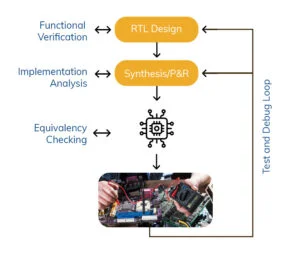
The FPGA Design development process can be broadly classified into three stages: design, verification, and implementation.
We center around moving our underlying idea or thought into an actual FPGA Design device in the design stage.
It involves commonly architecting the chip or separating it into smaller blocks to form an entire design.
We then, at that point, implement every one of these blocks utilizing an HDL language or another methodology.
In the implementation stages, the HDL design is converted into a programming file and further dumped on the FPGA Design.
FPGA Design Flow
The FPGA design flow comprises several steps, including design entry, synthesis, implementation, and device programming.
All these steps involved in the design flow are explained in detail below.

Design Entry
Schematics or Hardware Description Language (HDL) can be used for design entry.
Additionally, you have the option to mix the two and make the most of both by employing tools that can convert HDL to schematic and vice versa.
In general, when designing something that works with more sophisticated systems, it is preferable to use HDL.
You can avoid designing in lower-level hardware with this faster, language-based method.
For designers who specialize in hardware design, the schematic approach is an excellent option because it provides them with greater visibility.
Every strategy has advantages and disadvantages. Even if a schematic-based approach is simpler to read and understand, it is limited to smaller tasks.
However, HDL-based approaches are currently the most widely used design technique for FPGA design since they are quick and simple to use.
RTL Design and Simulation
The RTL design of a digital circuit is an intermediate representation that focuses on the operations performed on the data and the data flow between registers.
RTL simulation is used to verify the functionality and performance of the design before moving on to the synthesis and implementation stages.
Commonly used RTL simulation tools include ModelSim, XSIM, and VCS.
These tools enable functional and timing simulations, which help identify and address performance bottlenecks and design defects early on.
Synthesis
Once the design has been converted to code, it is synthesized, meaning that a circuit with gates, flip-flops, multipliers, and other components is created by translating the code.
The logic pieces and interconnects needed in the particular hierarchy are included in the netlist that is created from the HDL.
An HDL-based design syntax check kicks off the procedure.
After that, it is optimized by shrinking the design and getting rid of unnecessary and duplicate logic.
The final phase is planning out the technology to connect the design to the logic.

FPGA Design synthesis is carried out via specialized synthesis tools.
A large number of EDA firms, including Mentor Graphics, Cadence, and Synopsys, create tools for FPGA Design Synthesis.
Implementation
In the Implementation phase, the layout of the design is determined, and it consists of three steps:
- Translate
- Map
- Place & Route.
1) Translate

All of the input netlists are combined in this step to create the logic design file, which is stored as a.ngd file.
Here, the physical elements’ ports are assigned by the user-constrained file.
2) Map

This entails creating a.ncd file after translating the logic specified by the.ngd file into the FPGA components.
3) Place and Route

Here, routing joins the logic blocks by first inserting the sub-blocks from the previous phase into those blocks based on constraints.
The FPGA Design vendor provides the tool used in this step as they know how to translate the generated netlist into an FPGA.
The first step for the tools is to gather all the constraints set by the user and the netlist files.
These constraints contain the position of pins of I/Os and can include requirements regarding timing such as maximum delay, false path, etc.
Then the tool maps out the implementation by comparing the resource requirement specified in the files to the resources available on the FPGA Design being used.
The circuit is divided into logic blocks or elements in the form of sub-blocks. As a result, your entire design is placed in specific logic blocks and is ‘mapped out’ into the FPGA Design.
Testing and Debugging FPGA Designs
Testing and debugging are crucial steps in the process to ensure that the FPGA design functions as intended and meets performance requirements.
Common methods of testing include
Simulation: The design can be tested more quickly and precisely by using simulation tools to test it in a virtual setting.
In-circuit testing: Using a logic analyzer or oscilloscope to monitor signals and find problems when testing the FPGA design on the testbench or target hardware.
Tracking down and fixing issues related to functionality, performance, and resource consumption is part of debugging FPGA designs.
Using descriptive names for variables and signals makes code easier to read.
This is one of the finest debugging approaches. dividing the design into smaller, more manageable components through the use of a modular design approach.
Finding and isolating issues using simulation and in-circuit testing methods.
By following the FPGA design pipeline and utilizing best practices for testing and debugging, designers may create high-quality FPGA designs that meet the requirements of specific applications.
FPGA Program memory
FPGA programming, or the FPGA development process, is planning, designing, and implementing a solution to FPGA Design.
It all starts with a thought advancement, then turning the idea into a code. The RTL code is then simulated and debugged for functional verification.
After every one of the checks, the code is ready to download into the FPGA Design.
The FPGA Design development process can be broadly classified into three stages: design, verification, and implementation.
We center around moving our underlying idea or thought into an actual FPGA Design device in the design stage.
It involves commonly architecting the chip or separating it into smaller blocks to form an entire design.
We then, at that point, implement every one of these blocks utilizing an HDL language or another methodology.
In the implementation stages, the HDL design is converted into a programming file and further dumped on the FPGA Design.
FPGA Verification Process
When resolving design concerns before installing hardware in the lab, FPGA (Field-Programmable Gate Array) verification, including techniques like simulation and formal verification, is crucial.
Engineers can thoroughly test the FPGA design using simulation in a variety of scenarios, verifying functioning and assisting in the identification and correction of possible problems.
Comprehensive FPGA verification minimizes expensive and time-consuming hardware iterations, hence cutting down on error risk and expediting the time-to-lab phase.
In the end, this method produces hardware more quickly, at a reduced cost, and with greater development efficiency.
After the HDL code is written, there is a requirement to test it. This process is called verification.
Design Entry and Synthesis

Using a hardware description language (HDL) such as Verilog or VHDL, engineers produce a hardware description of the digital circuit at the start of the FPGA verification process, known as the design entry phase.
The logical components and connections of the FPGA are then represented by a netlist created from the design.
Simulation
Functional Simulation
- A crucial stage in the process is functional simulation, which entails utilizing simulation programs like ModelSim, XSIM, or Questa to confirm that the functionality of the design is proper.
- To mimic the design under varied input situations and conditions, engineers use test benches.
- This procedure aids in the identification of logical mistakes, functional validation, and assurance that the design serves the intended goal.
Timing Simulation
- By addressing the temporal characteristics of the design, timing simulation expands the verification process.
- It guarantees that the setup time, hold time, clock-to-q delays, and other necessary timing requirements are met by the design.
- Timing simulation guarantees that the design functions dependably at the intended clock frequency and assists in detecting possible timing violations.
Formal Verification
- In formal verification, a design’s correctness is established by mathematical proofs.
- Unlike simulation, it employs formal techniques to confirm that the design satisfies predetermined constraints or properties rather than depending on test vectors.
- This method is very helpful when it comes to confirming important design elements where thorough testing might not be possible.
Prototyping and Emulation
Implementing the design on a real FPGA or an FPGA emulator is known as prototyping.
It enables the design to be tested in real-time on actual hardware.
To verify the FPGA’s communication with the outside world, engineers can attach a variety of interfaces and peripherals to it.
By simulating every component of the FPGA-based system, including memory, peripherals, CPUs, and several FPGAs, emulation goes one step further.
This stage offers high confidence in the accuracy of the design and can identify problems with system-level interactions.
Lab Testing and Validation
To confirm its real-world performance, the lab physically tests the FPGA-based architecture.
In this step, the FPGA is frequently connected to external sensors, devices, and interfaces, and its behavior is verified in an actual setting.
Stress testing is another tool that engineers can use to test a design’s dependability in challenging circumstances.
Post-Implementation Verification
Post-implementation verification carries on validating the FPGA design in its operational context after it has been developed and deployed.
This stage could involve keeping an eye on the FPGA’s functionality, making sure it complies with safety and reliability regulations, and doing field testing to spot any unusual behavior.
Benefits of FPGA Verification
A crucial step in guaranteeing the dependability and functionality of digital architectures is FPGA verification.
The procedure provides several noteworthy advantages:
Early Bug Detection
Early identification of flaws and design faults is made possible by verification, particularly when formal methods and simulation are used.
Early problem-solving reduces the expense and work involved in rectification and avoids expensive post-production mistakes.
Functional Verification
It is possible to confirm that the FPGA design performs as anticipated using simulation.
To verify that the design satisfies the criteria and tests different facets of its functionality, engineers can build test benches.
Timing Verification
Timing simulation guarantees that the design satisfies the necessary timing limitations.
For FPGA designs that run at high clock frequencies and need exact timing to function properly, this is essential.
Formal Verification
A higher level of confidence in design correctness is provided by formal verification techniques like property and equivalency checking.
These techniques can confirm security features, safety-critical features, and other things that are difficult to check using simulation alone.
Prototyping and Emulation
Emulation and prototyping enable the concept to be tested in real-time on FPGA hardware.
This helps identify integration problems by illuminating the behavior of the design and how it interacts with external interfaces.
Lab Testing and Validation
The FPGA design is tested in a physical lab setting to make sure it functions as intended under real-world circumstances.
For safety-critical systems, where malfunctions could have catastrophic repercussions, it is especially crucial.
Stress Testing
Stress testing shows how the FPGA design functions under challenging or unforeseen circumstances.
It facilitates the discovery of flaws and vulnerabilities in the design, enabling enhancements.
System-Level Verification
System-level interfaces and interactions can be verified by lab testing and emulation.
For intricate FPGA-based systems with numerous FPGAs, processors, memory, and peripherals, this is essential.
Reduced Post-Production Costs
Determining and resolving design flaws in the verification stage considerably lowers post-production expenses and the likelihood of expensive recalls.
It also makes the development process run more smoothly.
Higher Reliability and Safety
Formal methods for functional safety verification improve the dependability and security of FPGA-based solutions.
This is especially important for applications where safety is crucial, like medical or automotive systems.
Accelerated Time-to-Market
Effective verification procedures guarantee that designs are fully tested and prepared for deployment, which helps to shorten time-to-market.
This is especially helpful in businesses with high competition where speed is essential.
Continuous Improvement
By detecting design flaws, tracking the FPGA’s performance after deployment, and utilizing the knowledge gained for subsequent projects, the verification process promotes continual progress.
FPGA Integration
The last but one step is termed system integration before the actual design.
The typical digital system being designed using FPGAs does not consist of a single FPGA Design.
Instead, it contains multiple FPGAs, glue logic such as PDLs or TTL parts, and other components such as EPROMs and SRAMs.
The model is near the real framework, and successful simulation shows that the physical prototype functions well.
Hardware Description Language(HDL) Design
All the levels of competence adopt areas of HDL application. The initial step is system specification, and afterward, the system is partitioned into two sections, software, and hardware.
The hardware can be ASIC, FPGA Design, or PLD (Programmable Logic Device).
Furthermore, for the system, the software acts as the mind of the equipment and makes it work appropriately.
 The fundamental limitation of the HDL language is that it cannot handle analog signals; it can take only digital systems.
Furthermore, the HDL models can be isolated in different abstractions like HDL (the highest level abstraction), then Gate Level, Netlist, and Layout (lowest level of abstraction).
The HDL hierarchy can be divided into various levels, as displayed in the figure underneath.
On the left side, we can see that the top module can be divided into two diverse sub-modules while the submodule can be further sub-partitioned into basic-level modules.
This can be better perceived while contrasting this and a model (FULL ADDER) on the right half of the figure underneath.

HDL Languages- VHDL and Verilog
Programming is done differently than with normal high-level languages since these FPGA building blocks are assembled into a circuit that will accomplish a specific task using a hardware description language.
Verilog and VHDL are the two most widely used languages for describing hardware.
VHDL: The verbose, strongly typed VHDL (VHSIC Hardware Description Language) language offers a high degree of abstraction, which facilitates the writing of complex designs. Europe and sectors like aerospace and defense use it extensively.
Verilog: Popular in the commercial sector and in the United States, Verilog is a more succinct, C-like language. Compared to VHDL, it has a lower level of abstraction, which can make complicated designs more difficult to work with but also provide the designer with more power.
Both languages have advantages and disadvantages, and industry standards or personal preference are frequently the deciding factors when choosing between VHDL and Verilog.
Related Post: Unerring Language: VHDL vs VERILOG
To understand better, How about we investigate these languages and see what the distinctions are?
VHDL
Hardware descriptions are written in the Very High-Speed Integrated Circuit Hardware Description Language (VHDL).
It is used to define digital and mixed-signal systems, including FPGAs (field-programmable gate arrays) and integrated circuits (ICs), in electronic design automation.
VHDL is a general-purpose parallel programming language that we can also employ.
To develop text models that explain or express logic circuits, we use VHDL.
A synthesis program processes the text model if it is included in the logic design.
A simulation program is incorporated into the procedure in the following stage to test the logic design.
In this step, we characterize the logic circuits that interface with the design by using the simulation models. This set of simulation models is what we call a testbench.
VHDL Functionality
These simulations alternate between two modes:
- Statement Execution: In this mode, the triggered statements are evaluated.
- Event Processing: During this mode, the events in the queue are processed.
Even if hardware designs are inherently identical, VHDL contains methods that can make the required modifications. These processes are not the same as the parallel processes in tasks (Ada) in terms of syntax.
Like Ada, VHDL is not case-sensitive and is a predefined portion of the programming language. Nevertheless, VHDL offers several features not found in Ada, such as a large collection of Boolean operators, such as NAND and nor. These extra capabilities allow VHDL to accurately model hardware-standard procedures.
Another advantage of VHDL is that it may be used as a general-purpose language for text processing because of its file output and input features.
However, a simulation testbed is usually where we see them being used for stimulus or data verification.
A testbench for functionality verification designs can be written in VHDL using files on the host computer to compare expected outcomes, set stimuli, and allow user involvement. Certain VHDL compilers create executable binaries.
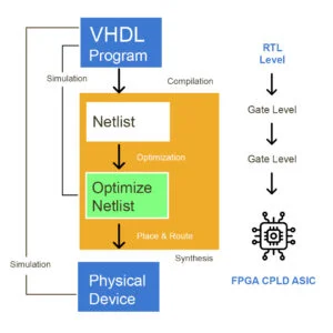
VHDL Design Flow
The VHDL design flow begins with writing the VHDL program.
Leading manufacturing companies such as Xilinx and Altera provide proprietary software development tools like Xilinx ISE and Altera Quartus.
These tools enable editing, compiling, and simulating VHDL code. Within VHDL, circuits are described at the RTL (Register Transfer Level).
The VHDL code is compiled, resulting in a netlist at the gate level.
During this process, the compiler translates the high-level VHDL RTL code into gate-level representations.
The netlist is further optimized to achieve an optimized netlist at the gate level.
This optimization aims to improve speed and reduce space utilization. Simulation of the design occurs at this stage.
After optimizing the Netlist using place-and-route software (fitter), the VHDL design is implemented on CPLD/FPGA or prepared as a final MASK for ASIC. Subsequently, the final device undergoes simulation and verification
In addition to serving as a digital circuit design tool, VHDL functions as a programming language with its own program structure, akin to other languages such as C
VERILOG
Learning Verilog itself is not a troublesome task, yet making a good design can be. In any case, we center around straightforward designs here and will make an honest effort to clarify things as essential as they can be.
If you are accustomed to procedural languages such as C, and C++, you will have to comprehend that not all things happen consecutively in the digital world. Many things happen parallelly as well. C programs run on microprocessors, which execute each instruction in turn successively.
Let’s look at the overview of Verilog and some design guidelines that can be followed while executing a design.
Coding style significantly affects how an FPGA configuration is carried out and eventually how it performs.
Albeit numerous well-known Synthesis tools have fundamentally further developed improved optimization algorithms for FPGAs, the architect still must produce HDL code that guides the synthesis tools and accomplish the best result for a given design. This section gives Verilog HDL design rules for both amateur and experienced planners.
 Fundamentally, Verilog is all about creating modules, interconnecting them, and managing the timing of interactions.
An HDL design can either be synthesized as a flat module or as many small hierarchical modules.
Each methodology enjoys its benefits and inconveniences. Since design in smaller blocks is simpler to monitor, applying hierarchical structure to large and complex FPGA design is the best approach.
The hierarchical coding methodology allows a group of engineers to work on one design simultaneously.
It speeds up the design compilation process and reduces the design period by permitting the re-utilization of design modules for current and future designs.
Verilog can represent the hierarchy of a design. The Verilog structures which are used to build the hierarchy are
- modules
- ports
A Verilog model is made out of modules. A module is the fundamental unit of the model, and it may be composed of instances of other modules. A module made out of other modules is known as a parent module, and the instances are called child modules.
 In this example, there are four modules: system, comp_1, comp_2, and sub_3. The system is the parent of comp_1 and comp_2, and comp_2 is the parent of sub_3. comp_1 and comp_2 are the children of the system, and sub_3 is the child of comp_2.
A module is defined as shown below

The is the type or name of this module. This is the list of ports connected to the module.

Here are some tips for building hierarchical structures:
- The top level should only contain instantiation statements to call all major blocks.
- Any I/O instantiations should be at the top level.
- Any signals going into or out of the devices should be declared as input, output, or bidirectional pins at the top level.
Port Connections at Instantiations In Verilog
There are two ways of specifying connections among ports of instances.
A) By ordered list (positional association)
This is the more intuitive method. The connected signals must appear in the module instantiation in the same order as the ports listed in the module definition.
B) By name (named association)
When there are too many ports in a large module, it becomes difficult to track the order. Connecting the signals to the ports by the port names increases readability and reduces possible errors.

Verilog Parameters and its Instantiations
In Verilog, parameters are constants and do not belong to other data types such as register or net data types.
A constant expression refers to a constant number or previously defined parameter. We cannot modify parameter values at runtime, but we can change a parameter value using the defparam statement.
The defparam statement can modify parameters only at the compilation time. Parameter values can be adjusted using # delay specification with module instantiation.
The values of parameters can be overridden during instantiation so that each instance can be customized separately. Alternatively, a defparam statement can be used for the same purpose.
 Terminologies and basic concepts
Before going deep down into the Verilog coding styles, let us look at some of the terminologies and basics related to HDL coding.
Reg and wire
Data types in Verilog are divided into NETS and Registers. These data types differ in how they are assigned and hold values, and also they represent different hardware structures.
NETS –
The net variables represent the physical connection between structural entities. These variables do not store values(except trireg); they have the value of their drivers, which changes continuously by the driving circuit. Some net data types are wire, tri, wor, trior, wand, triand, tri0, tri1, supply0, supply1, and trireg. The wire is the most frequently used type. A net data type must be used when a signal is:
- driven by the output of some device.
- Declared as an input or in-out port.
- On the left-hand side of a continuous assignment.
Registers –
The register variables are used in procedural blocks, which store values from one assignment to the next. An assignment statement in a procedure acts as a trigger that changes the value of the data storage element. Some register data types are reg, integer, time, and real. Reg is used for describing logic, integer for loop variables and calculations, real in system modules, and time and real-time for storing simulation times in test benches.
Remember –
- The reg variables are initialized to x at the start of the simulation. Any wire variable not connected to anything has the x value.
- The size of a register or wire may be specified during the declaration.
- Register and wire are declared as vectors when the reg or wire size is more than one bit.
- The Verilog HDL value set consists of four fundamental values:
 Structured Procedures
There are two structured procedure statements, namely initial and always. They are the introductory statements for behavioral modeling from which other behavioral statements are declared. They cannot be nested, but many of them can be declared within a module.
a) initial statement
The initial statement executes precisely once and becomes inactive upon exhaustion. If there are multiple initial statements, they all start to run concurrently at time 0.
b) always statement
The always statement continuously repeats itself throughout the simulation. If there are multiple always statements, they all start to execute concurrently at time 0. Always statements may be triggered by events using an event-recognizing list @( ).
Task and Function
Tasks and functions in Verilog closely resemble the procedures and functions in programming languages.
- Both tasks and functions are defined locally in the module in which they will be invoked.
- No initial or always statement may be defined within either tasks or functions.
- Tasks and functions are different – tasks may have 0 or more arguments of type input or output; function must have at least one input argument.
- Tasks do not return values but pass values through output and input arguments; functions always return a single value but cannot have output or input arguments.
- Tasks may contain delay, event, or timing control statements; functions may not.
- Tasks can invoke other tasks and functions; functions can only invoke other functions, but not tasks
 Sequential & Parallel Blocks
Block statements group multiple statements together. Block statements can be either sequential or parallel. Block statements can be nested or named for direct access and disabled if named.
a) Sequential block
Sequential blocks are delimited by the pair of keywords begin and end. The statements in sequential blocks are executed in the order they are specified, except for nonblocking assignments.
b) Parallel block
Parallel blocks are delimited by the pair of keywords fork and join. The statements in parallel blocks are executed concurrently. Hence, the order of the statements in parallel blocks is immaterial.
Assignments
a) Continuous assignment
 Continuous assignments are always active — changes in RHS (right-hand side) expression are assigned to LHS (left-hand side) net. LHS must be a scalar or vector of nets, and assignment must be performed outside procedure statements.
Delay may be associated with the assignment, where new changes in expression are assigned to the net after the delay. However, note that such delay is called inertial delay. The 1st change within the delay is not assigned to the net. If the expression changes again within the delay, the last change is only enacted and assigned to the net.
b) Procedural assignment
LHS must be a scalar or vector of registers, and assignment must be performed inside procedure statements (initial or always). The assignment is only active (evaluated and loaded) when control is transferred to it.
After that, the value of the register remains until another procedural assignment reassigns it.
There are two types of procedural assignments:
- Blocking assignment
Blocking assignments are executed in the order specified in the sequential block, i.e., a blocking assignment waits for the previous blocking assignment of the same time to complete before executing.

- Nonblocking assignment
Nonblocking assignments are executed concurrently within the sequential blocks, i.e., a nonblocking assignment executes without waiting for other nonblocking assignments to occur at the same time to complete.
 Timing Controls
a) Delay-based
Execution of a statement can be delayed by a fixed time period using the # operator.
 Intra-assignment delay
This evaluates the RHS expression immediately but delays for a fixed period before assigning it to LHS, which must be a register.
 b) Event-based
Execution of a statement is triggered by the change of value in a register or a net. The @ operator captures such a change of value within its recognizing list. To allow multiple triggers, use, or between each event.
Level-sensitive
The @ is edge-sensitive. To achieve level sensitivity, use additional if statements to check the values of each event.
 Alternatively, the combination of always and wait can be used. However, note that wait is a blocking statement, i.e., wait blocks the following statement until the condition is true

c) Named-event
The event is explicitly triggered (with -> operator) and recognized (with @ operator). Note that the named event cannot hold any data.
 Conditional Statements
The body only allows a single statement. If multiple statements are desired, block statements may be used to enclose various statements in place of the body.
a) If-Then-Else

b) Case

c) Loop Statements
The body only allows a single statement. If multiple statements are desired, block statements may be used to enclose multiple statements in place of the body.
a) While

b) For

c) Repeat
Iterations are based on a constant instead of a conditional expression.

d) Forever

After getting such a detail about VERILOG, I guess we are good to get our hands on with Verilog. Let us design a NOT gate in Verilog, simulate it, and make it ready to test on real hardware. A NOT gate (an inverter) is the simplest of all gates.
The output of an inverter is the negation of the input. i.e., B = !A, where A is the input and B is the output. The below table summarizes the behavior of NOT gate as a truth table.
 “NOT” gate can be considered a module with one input and one output with an internal behavior of B=!A. The graphical representation of the inverter module is shown below.

Let us see how we would represent this in Verilog.

Extremely basic, right? Let us scan through every single line and attempt to get what is happening in this code snippet.
The name of the module is “my_module” and is declared using the “module” keyword. The keyword module in Verilog defines our module (called my_module) and assigns two ports to it. Everything that goes into this module is placed in between the “module” and “endmodule” keywords. “my_module” has two ports. The ports’ size or direction is not known yet.
In the next line, Port A and Port B are declared as input and output. Finally, an assign statement is used to get the desired output.
Ok, so now we have a module ready, let’s run a simulation on the module and see if it works as expected. To simulate the module, we need to give input to the module. The input is given through a test bench.
The test bench is designed to generate the necessary inputs for the module under analysis (Here “my_module”). A test bench is nothing but another Verilog module that generates some signals and feeds them to the module under test.
The test bench should be a “top module” (top-level module) with no I/O ports during the simulation. But when it comes to implementation on a real FPGA, the “top module” can have I/O ports, and test benches won’t be the top modules there. So here goes the test bench code.
 Let me break this down for you.
The test bench is just another module with no I/O ports, as mentioned earlier. A wire named “out” and a reg named “clock.” is created. A clock is created on reg “clock” by periodically inverting it and feeding it to the input (port A) of my_module. The wire “out” is connected to the output port (port B) of my_module.
The result should appear on the wire “out” in the simulation.
The “always” block will keep on executing as long as the simulation runs.
In the “always” block, the reg “clock” is inverted after every one-time unit delay. The symbol # is a way to specify a delay in Verilog. So the always block executes throughout till the code is running. The clock inside the always block is inverted continuously to generate the square wave. Remember that the # symbol is not a synthesizable element. We have to find another way (using flip-flops) if a delay is needed in the design. But it works just fine for simulation.
The next block is an initial block. As already explained above in the section “Terminologies and basic concepts), this block will be executed only once at time t = 0. So anything that we need to initialize should go here. The initial block also is usually used only in test benches.
Initial blocks are rarely used in a synthesizable code; reset logic is created if initialization is required. We initialize the reg “clock” to zero. This is very important. If we don’t initialize a register, its value is unknown, and no matter how many times an unknown is inverted, the result will always be unknown. That is, if we leave “clock” uninitialized, “clock” won’t be generated.
The last part of the initial block is the $finish directive. The $finish directive is placed after a 10-time unit delay; this means after simulating the design for 10-time units, the stimulator will stop running.
Last but not least, the module instantiation. The statement “myModule notGate(clock, out)” creates an instance of the module “myModule” with the name “notGate.” You can create as many instances as you want from a module. One crucial thing here is the wiring. If you look at the code, you can see the reg “clock” placed as the first parameter, and the wire “out” is set as the second parameter.
The reg “clock” is connected to port A of the module instance, and wire “out” is connected to port B.
Now both testbench, as well as the module to be tested, is ready. It would help if you had an HDL simulator to simulate it. Simulators such as ISE Simulator, ModelSim, and Questa, etc., are available.
While simulation can tell us many things about the correctness of our module, there is nothing like putting it on a piece of hardware and seeing it working. To run the design on the actual board, we need to synthesize it and implement it on the hardware.
As mentioned earlier, the test bench code is used only for simulation. To synthesize our module, we have to remove the test bench code. As discussed earlier, HDL Synthesis is the step where the HDL ( Verilog/VHDL or any other HDL for that matter) is interpreted, and an equivalent hardware topology is generated. This hardware topology will be particular to the target FPGA Design selected.
Let’s come back to our module and think about how we can implement the same on the hardware. As we know, the output of a NOT gate is always the negation of the input. We can have many possible hardware configurations to test this module. The easiest would be with a switch and an LED. See the proposed hardware configuration in the picture below.

In the above diagram, a switch is connected to an input pulled up to VCC using a resistor. The output is connected to an LED.
When the switch is in the open position, there will be a positive voltage, i.e., a logic “1” at the input (A) of the NOT gate.
That means the output (B) will be at logic “0”. So the LED will be in OFF condition.
When the switch is closed, the input of the NOT gate will become logic “0,” and the output will switch to logic “1” state. And the LED will glow.
Now we know the basic hardware requirements.
We need the following in our prospective hardware.
- An input-capable IO with a pull-up resistor and a switch attached.
- An output-capable IO with an LED connected.
You can select any FPGA Design board to test this module’s functionality. We now have a Verilog module that we want to implement, and we have selected a hardware platform and decided what IOs to use for implementation.
The module to be tested has two ports—Port A, the input, and Port B, the output. Now an obvious question would be arising – how are we going to attach Port A to the specific pin (switch) of the hardware and Port B to the particular pin (LED) of the hardware?
It is done by defining user constraints. User constraints tell the router and the placement logic (part of the HDL synthesizer) on which physical pins the module signals are connected. A list of constraints is made, placed in a file, and is included t in the project. This file is called a User Constraints File.
For The Radiant tool, it is the .pdc file, and for Xilinx, it is the .ucf file.
After writing the user constraint file, a bitstream file is generated and dumped onto the selected board using the programmer tool. The functionality of the module is tested.
Coding Guidelines
Below are the coding style rules that prove to be the most beneficial. Note that these are recommended for both VHDL and Verilog to keep consistency. There are three main benefits to adopting the coding style below.
- Increased readability of code
- Improved thoughtfulness of code writing
- Code is less error-prone
Prefixes

i_ and o_ prefix
An essential style you should adopt! Too many designers do not indicate if their signals are inputs or outputs from an entity/module.
It can be challenging and annoying to look through the code to determine the direction of a signal. Additionally, a signal named “data” and its output will be much harder to find in your code via a search than a signal named “o_data.” Examples: i_address, o_data_valid.
r_ and w_ prefix
This is the second most crucial style you need to use. Indicating if your signal is a register or a wire is hugely vital to writing good code.
Verilog is nice because it forces you to declare your signal as a reg or a wire, but VHDL has no such requirement! Therefore this style is essential for VHDL coders.
All signals declared with r_ should have initial conditions. All signals declared with w_ should never appear to the left-hand side of an assignment operator in a sequential process (in VHDL), or a clocked always block (in Verilog). Examples: r_Row_Count, w_Pixel_Done.
c_, g_, and t_, prefix
These are helpful indicators when coding. c_ indicates that you are referring to a constant in VHDL or a parameter in Verilog. g_ is used for all VHDL generics. t_ demonstrates that you are defining your own data type
Examples: c_NUM_BYTES, t_MAIN_STATE_MACHINE.
All capital letters are used to define states in state machines. e.g., IDLE, DONE, CLEANUP.
Capitalization Keynote
Whether or not you want to capitalize your signal names is up to you.
Whatever you choose, stay consistent! VHDL is not case-sensitive, so r_ROW_COUNT is the same as r_Row_Count, but this is not true in Verilog.
Verilog is case-sensitive, so maintaining rules about capitalization is very important! You don’t want to accidentally create two different signals when you meant to make just one signal.
Initializing Signals Keynote
There is a fairly widespread misconception that FPGAs need to have a reset signal into a register to set an initial condition.
This is not true; FPGA Design registers can have initial values. All FPGA Design registers can be initialized to zero or non-zero values.
It’s best practice to reset as few Flip-Flops as possible in your design and to rely on initializing all Flip-Flops instead.
The reason for this is that each reset line you add to a Flip-Flop takes routing resources and power and makes your design harder to meet timing.
The rule you should be following is this: All registers (as identified by r_ prefix) should always have an initial condition applied to them.
No wires (as identified by w_ prefix) should EVER have an initial condition applied to them.
Based on the design requirement, every design on board has to run at a certain specified speed. There are generally three types of speed requirements in any FPGA design:
Timing requirement – How fast or slow a design should run. Target clock period (or clock frequency) and other constraints are required to define the design speed.
Throughput – The average rate of the valid output delivered per clock cycle
Latency – the amount of time required when the valid output is available after the input arrives, usually measured in the number of clock cycles
Throughput and latency are usually related to the design architecture and application, and they need to be traded off based on the system requirement.
For example, high throughput usually means more pipelining, which increases the latency; low latency usually requires longer combinatorial paths, which removes pipelines, reducing the throughput and clock speed.
FPGA Design designers often struggle to meet the timing requirement to ensure that the design runs at the required clock speed. It can require hard work for high-speed design to close timing using various techniques (including the trade-off between throughput and latency, appropriate timing constraint adjustments, etc.) and running through multiple processing iterations, including Synthesis, MAP, and PAR. Said that, let’s jump to the last topic of the discussion.
Advantages of FPGA
FPGAs have a special set of benefits, especially when it comes to adaptability and flexibility. Let’s examine these advantages in greater detail:

Better Performance
- Performance is one of FPGA’s primary benefits. Because a typical CPU cannot process data in parallel, FPGAs have an advantage over CPUs because they can process data faster and calculate data in parallel.
- An FPGA with careful design can perform any function more quickly than a CPU running software code in sequence.
- Flexible and programmable, FPGAs are made possible by extra gates and wiring. FPGAs operate more slowly than ASICs because of this overhead, which is expensive.
Programmability
- The most significant benefit that FPGAs possess over all other options is their reprogrammability.
- This implies that FPGAs can still be updated, changed, and modified to perform entirely different tasks from those for which they were originally intended, even after the circuit has been designed and put into use.
- Reprogrammability lowers the effort and expense needed to maintain these chips over time.
- When hardware ages, you can simply update its code and program it in the field with the new functionality, saving you money on redesigning or replacing it.
Cost Efficiency
- Even though FPGAs may have higher unit costs, they prove to be extremely cost-effective in the long run because they can be reprogrammed repeatedly.
- This is undoubtedly one benefit of FPGA architecture. They relieve you of the obligation to pay for ongoing expenses related to bugs that you might be forced to pay if you choose to use an ASIC.
- In addition to the fact that designing or configuring an FPGA chip does not require the use of expensive tools, ASICs incur significant one-time costs that are completely avoided in the case of FPGAs.
- In the long run, ASICs also prove to be more costly because hardware redesigns are required whenever updates and improvements are required. FPGAs don’t split these expenses because reprogramming them costs almost nothing.
Parallel Task Performance
- Sequential data processing chips are typically not utilized in applications where timing is of the essence. It is possible to design FPGAs with multiple blocks that process data simultaneously. This implies that it can provide time-critical data processing and much higher scalability when compared to other processors like ASICs and MCUs.
Prototyping
- The reprogrammable and reusable nature of FPGAs is one of their advantages, as previously mentioned. They are therefore the ideal option for prototyping, particularly for ASIC validation.
- It is crucial to ascertain whether your ASIC design is operational and effectively fulfills its intended purpose before you tape it out.
- Because ASICs are very expensive and difficult to make, you will have to spend a lot of time and money redesigning the ASIC if your chip needs to be modified.
- The reprogrammability feature of FPGAs lets you run test runs by adjusting the programming and figuring out the best setup on a single chip. It is simple to turn the FPGA into a permanent ASIC and put it to use once prototyping is finished and the optimal course of action has been established.
Faster Time to Market
- One of the biggest benefits of FPGAs is that they enable you to complete product development quickly, which reduces the time it takes to market. There is not much of a learning curve and FPGA design tools are simple to use.
- Furthermore, HDL, a higher description language that is also a modular programming code, is used to design FPGAs. Designing with HDL code such as Verilog or VHDL makes the process incredibly quick and effective.
- Reprogramming FPGAs at the software level to test and validate the design in the lab is very simple. Fast modification times enable bug fixes to be implemented in brief cycles.
Simpler Design Cycles
- FPGAs have simpler design cycles than ASICs, which means that the design tools handle the majority of the work, such as placement, routing, and timing regarding the specifications you’ve set for it.
- As a result, when transforming the program code into a downloadable design, they practically never need human intervention.
- If the design does not work as planned, a new downloadable code can be created in a few hours, simplifying and expediting the entire design cycle.
Adaptability
- Reprogrammable FPGAs allow you to change and adapt at the customer level instead of having to rebuild the product every time an update is required.
- Even once the product has been designed, developed, and delivered, it can easily be updated and tailored to the needs of the client.
Real-Time Application
- As previously mentioned, the more efficient processing architecture of FPGAs makes them ideal for time-critical systems.
- Because they can process more data faster than other market options, they are perfect for real-time applications.
System on Chip
- The number of gates on FPGAs has increased since the 1990s. This allowed for the inclusion of custom hardware code and CPU cores, ranging from one to many cores, inside the FPGA.
- FPGAs work as a system on the chip by integrating hardware code and CPU cores into a single chip.
Disadvantages of FPGA
When compared to other technologies like ASICs and microcontrollers, FPGAs have a few drawbacks. A few of the drawbacks include:
Cost
- FPGAs can cost more than ASICs or microcontrollers, particularly when producing large quantities.
- In large volumes, the cost per unit of an FPGA is typically higher than that of an ASIC or microcontroller.
Power consumption
- Power-sensitive applications may be concerned because FPGAs often use more power than ASICs and microcontrollers.
Design complexity
- The design process for FPGAs can be more complex than for microcontrollers, requiring specialized knowledge of hardware design, HDL, synthesis, and place-and-route tools.
Performance limitations
- While ASICs are specially developed for a particular purpose and can be highly optimized for performance, FPGAs may not be as fast as ASICs for some operations, even if FPGAs enable parallelism and can deliver high performance for some workloads.
Size
- Compared to comparable ASICs or microcontrollers, FPGAs may have bigger dimensions because they have more resources for reconfiguration and programmability.
Configuration time
- When compared to ASICs and microcontrollers, FPGAs can take longer to startup because they need to be configured first.
FPGA Vs ASIC Vs PLD vs. microcontroller
Digital logic functions can be implemented using a variety of technologies, including FPGAs, microcontrollers, Programmable Logic Devices (PLDs), and Application-Specific Integrated Circuits (ASICs). Now let’s examine these technologies in more detail:
FPGAs
- FPGAs can be reprogrammed, as was previously indicated, which makes them appropriate for a variety of uses.
- Compared to ASICs, PLDs, and microcontrollers, they can be more costly and power-hungry, but they can offer higher performance and parallelism.
ASICs
- ASICs have optimum performance and power consumption because they are specially designed for a given application.
- They are appropriate for high-volume manufacturing runs, but they have significant upfront costs, require a long time to build, and lack the flexibility of FPGAs and PLDs.
Related Post: FPGA VS ASIC Design [Comparison]
PLDs
- Similar to FPGAs but less sophisticated and resource-hungry, PLDs, such as sophisticated Programmable Logic Devices (CPLDs) and Simple Programmable Logic Devices (SPLDs), are reconfigurable hardware.
- They can be less expensive and power-hungry than FPGAs, making them ideal for simpler digital designs.
- However, in more complicated applications, they could not have the same performance and flexibility as FPGAs.
Related Post: CPLD VS FPGA – All you need to know
Microcontrollers
- General-purpose computing devices with integrated input/output, computation, and memory are called microcontrollers.
- Compared to FPGAs and PLDs, they are generally less parallel and slower, but they are less expensive, require less power, and are simpler to program.
Related Post: FPGA vs. Microcontroller: Battle of Embedded Systems
In conclusion, microcontrollers are inexpensive and simple to design for, ASICs offer optimum performance and power consumption, PLDs offer simplicity and cost-effectiveness, while FPGAs offer flexibility and parallelism.
The particular needs of the application and the intended trade-offs between performance, power consumption, development time, and cost determine which technology is best.
FPGA Applications
Field-Programmable Gate Arrays (FPGAs) are versatile integrated circuits that can be configured and reconfigured to implement a wide range of digital circuits and functions. Here are some common applications of FPGAs:
Aerospace & Defense

- Field programmable gate arrays, or FPGAs, are crucial to the defense and aerospace sectors.
- The primary uses of FPGA in aerospace and military include signal processing, radar systems, avionics, cybersecurity, UAVs, electronic warfare, testing, and space exploration.
- It also provides a high-performing, adaptable, and flexible solution that ensures systems stay relevant through upgradability without necessitating complete hardware overhauls.
Automotive

- FPGAs enable improvements in automobile technology related to safety, performance, and communication.
- In addition to providing real-time processing for ADAS, they also help with sensor fusion and crucial processing for autonomous driving.
- FPGAs facilitate V2X communication customization, infotainment, and functional safety in addition to power efficiency and cybersecurity.
- Their adaptability and reconfigurability will play a major role in shaping the future development of automotive systems.
Data Center

- Field-Programmable Gate Arrays, or FPGAs, are becoming more and more used in data centers due to their ability to process data in parallel, energy efficiency, and customization choices.
- Network function virtualization, accelerated processing, and improved security via accelerated cryptography are all applications for FPGAs.
- They also provide reduced latency and dynamic reconfiguration. Complex programming and cost considerations present difficulties.
- As programming tools and technology progress, FPGAs are expected to play an increasingly important role in data centers by providing improved performance, energy efficiency, and creative data processing.
Medical

- An increasing number of applications are leveraging FPGA design to handle biomedical pictures generated by PET treatments, CT scans, X-rays, three-dimensional imaging, and other modalities.
- Frequency is beneficial because more and more medical vision systems require higher processing speeds and resolutions, and many of them need to be created in real time.
- FPGA design and parallel processing are perfect for addressing these requirements.
Video and Image Processing

- FPGAs are necessary for processing photos and movies since they handle data concurrently through the use of parallel processing.
- Their flexible architecture, which optimizes speed and resource use, makes them ideal for real-time applications like as streaming and medical imaging.
- FPGAs are great at object detection, video compression, and image enhancement.
- They also speed up deep learning inference. Their adaptability allows for a greater variety of I/O and camera interfaces, which facilitates system integration.
Digital Signal Processing

- FPGAs, or field-programmable gate arrays, are indispensable to digital signal processing (DSP) due to their reconfigurability and capacity for parallel processing.
- Common applications include biomedical signal processing, digital filters and transformations, sonar and radar systems, software-defined radio, image and video processing, real-time signal processing, and speech and audio processing.
- FPGAs thrive in many domains where high-performance and configurable signal processing is required because they allow sophisticated algorithms to be executed in real-time and parallel.
Wireless Communications

- Field-programmable gate arrays, or FPGAs, are revolutionizing wireless communications with their unparalleled flexibility and adaptability.
- The reconfigurable feature of these devices facilitates the swift implementation of various communication standards, including LTE and 5G.
- Additionally, their parallel computing capabilities enhance real-time processing speed and throughput.
- FPGAs are successful in baseband processing, MIMO systems, Software-Defined Radio, and cognitive radio applications.
FPGA Design Examples and Applications
Digital Signal Processing (DSP) with FPGAs
Digital signal processing (DSP) involves the analysis and manipulation of digital signals, such as audio, video, and sensor data.
FPGAs are perfect for DSP applications because of their flexibility and parallelism. Applications of FPGA-based DSP comprise, for example:
- Audio processing: FPGAs are useful for compression, equalization, noise reduction, and audio effects.
- Image processing: Real-time image processing tasks such as object recognition, edge detection, and filtering can be carried out by FPGAs.
- Software-defined radio (SDR): Several radio communication protocols can be implemented using FPGAs, allowing for extremely flexible and customizable radio systems.
FPGA-based Artificial Intelligence (AI) Machine Learning (ML)

FPGAs are crucial in AI and ML applications because of their advantages such as low latency, fast throughput, and energy economy.
Several artificial intelligence and machine learning initiatives that make use of FPGAs are as follows:
- Deep learning accelerators: Compared to conventional CPU and GPU-based solutions, FPGAs can improve performance and save power consumption by speeding up the training and inference of deep neural networks.
- Edge AI: By enabling AI processing at the edge, FPGAs decrease the amount of data that needs to be transmitted to the cloud while enhancing security and privacy.
- Custom AI hardware: Custom AI algorithms that are suited to particular applications can be implemented using FPGAs, improving both performance and power efficiency.
Benefits of FPGAs in AI-based Applications
1. Parallel Processing Capabilities
- FPGAs are excellent at parallel processing, making it possible to carry out several operations at once.
- For AI algorithms, which frequently require intensive matrix operations and neural network computations, this parallelism is quite advantageous.
2. Low Latency and High Throughput
- Due to their ability to directly implement hardware circuits, FPGAs can provide low-latency and high-throughput performance.
- As a result, they are appropriate for real-time AI applications like autonomous driving or video analytics where prompt responses are essential.
3. Flexibility and Re-programmability
- FPGAs have many reprogramming capabilities that let designers modify their hardware designs in response to shifting specifications.
- This adaptability is advantageous in the quickly changing field of artificial intelligence, where algorithms and models often go through upgrades and improvements.
FPGAs in Networking and Communication

FPGAs are frequently utilized in networking and communication systems because of their exceptional performance, versatility, and adaptability.
Several examples of FPGA-based networking and communication projects are listed below:
Network switches and routers: High-performance, low-latency ethernet switches and routers can be implemented with FPGAs, facilitating quicker and more effective data transfer.
Optical communication: FPGAs can be used to implement high-speed data transmission and signal processing in optical communication systems such as dense wavelength division multiplexing (DWDM).
Wireless communication: Several wireless communication protocols, including Bluetooth, Wi-Fi, and 5G, can be implemented using FPGAs, allowing for flexible and customizable communication systems
The following are some of the features of an FPGA that make it a suitable choice for processing power.
- Parallel Processing – One of the advantages of FPGAs that make them a decent choice for working with measurement systems and other computing applications that require processing a large amount of data is that they can process in parallel. In contrast, CPUs work sequentially, making it not a practical choice.
- FPGAs Perform Time-Critical Processing – Being able to process data parallelly, FPGAs have low latency, making them suitable for applications requiring very time-critical calculations such as in software-defined radio, medical devices, and mil-aero systems.
- FPGAs Have Optimal Performance per watt – When compared with a CPU or GPU, one will get better per watt performance with an FPGA. This low power consumption can be almost 3 to 4 times less than that of a GPU. The operating cost of an ASIC is by a long shot the best, but the high initial price does a ton to counterbalance that.
Best Practices for FPGA Design
The general best practices for FPGA design will be covered in this section, with an emphasis on modularity, readability of code, and methods for performance, power, and resource optimization.
Code Readability and Modularity
Efficient FPGA design requires maintaining the modularity and readability of the code. You may make your designs more scalable and maintainable by adhering to these guidelines:
- Descriptive naming: To improve the readability of your code, give signals, variables, and modules meaningful names.
- Comments: If your code performs complicated or obscure tasks, make sure to include comments outlining its functionality and goal.
- Modularity: Break your design into smaller, more manageable modules or components. This approach makes it easier to debug, maintain, and reuse code.
Optimizing FPGA Designs for Performance, Power, and Resource Usage
You may attain the ideal balance between performance, power consumption, and resource usage by optimizing your FPGA design. Among the optimization methods are:
- Pipelining: Divide complicated tasks into smaller steps and execute them concurrently to boost throughput and lower delay.
- Resource sharing: To save space and power, reuse hardware resources for numerous tasks, such as memory blocks, multipliers, and converters.
- Clock gating: If you want to lower dynamic power usage, disable the clock domain signal in any unused or idle parts of your design.
Use the optimization features offered by synthesis and implementation tools, like as Xilinx Vivado and Intel Quartus, in addition to these methods.
With the use of these tools, you may make the most of your unique design restrictions and requirements while still getting the greatest outcomes.
You can produce excellent, effective designs that satisfy the requirements of your particular applications by adhering to best practices for FPGA design and using optimization techniques.
Frequently Asked Questions (FAQs)
Q: Why is FPGA used?
ASICs are made for specific tasks; field-programmable gate arrays, on the other hand, can be reprogrammed.
Using a field-programmable gate array, computer users can tailor the capabilities of microprocessors to their requests. FPGAs are used by engineers to build specialized integrated circuits.
Q: What are the two types of FPGA?
Classifying FPGAs: Different Types
- High-End FPGAs – These FPGAs have a high gate density, making them more complex than mid-range FPGAs.
- Low-End FPGAs – These FPGAs use less power than high-end and mid-range FPGAs and are less complex due to fewer gates.
Q: What is FPGA best for?
FPGAs are frequently utilized in situations where low-latency data transmission across several networks is required.
They’re highly helpful in getting rid of memory buffering and getting over I/O bottlenecks, which are among the biggest things impeding the performance of AI systems.
FPGAs can expedite the AI workflow from start to finish by speeding up data ingestion.
Q: What is the advantage of FPGA?
An FPGA’s primary benefit over an application-specific IC (ASIC) or comparable discrete circuit is its ease of functional modification after a product has been designed.
Furthermore, compared to an equivalent discrete circuit, FPGA can be more energy-efficient and need less board area.
Q: Is FPGA hardware or software?
Adaptive hardware, which has the rare capacity to be changed after construction, is the foundation of FPGA technology.
Every hardware block in an array is programmable and can be joined in any way required to create highly effective, application-specific structures.
Q: What are the steps in FPGA design?
Functional Design, Synthesis, Place & Route, Integration, and Fabrication are the five primary phases.
Before going on to the next step, each stage includes a full generate-simulate cycle in which the design components are generated and then simulated to guarantee proper functioning.
Q: What is FPGA architecture?
A programmable logic block array coupled to one another via a programmable interconnect network makes up an FPGA.
An underlying programming technology allows for FPGA programmability. First, this chapter goes over various programming technologies in brief.
Q: Where is FPGA used?
FPGAs are frequently used in research and development and restricted (low) production of customized goods, where the greater cost of individual FPGAs is not as significant and when designing and producing a custom circuit would not be practical.
Q: What is the practical use of FPGA?
Here are some examples of actual use cases:
Processing of digital signals (DSP): Wireless communication, audio processing, picture and video processing, and other high-performance DSP applications are among the many uses for FPGA.
Their reconfigurability and capacity for parallel processing make them perfect for real-time signal processing.
Q: What is the principle of FPGA?
Reprogrammable integrated circuits with a variety of programmable logic blocks are called field-programmable gate arrays, or FPGAs.
The adoption of FPGA chips is fueled by their parallelism, hardware-timed speed dependability, and flexibility.
Q: Is FPGA a microcontroller?
An FPGA is a digitally integrated circuit that is highly programmable, enabling the user to design unique digital circuits, while a microcontroller is a more application-specific, general-purpose device that is mostly software-adjustable.
Q: What language is used in FPGA?
One of the most popular programming languages for FPGAs is Verilog.
It is a hardware description language (HDL) intended for use in digital circuit design and verification.
Verilog is a text-based language that makes it simple for users to explain how their digital circuits behave.
Q: Is FPGA a processor?
While CPUs are meant to be general-purpose devices that can be programmed to do a wide range of functions, FPGAs are extremely adaptable and can be reprogrammed to execute any digital function.
Q: Which RAM is used in FPGA?
Now, blockrams and distributed RAMs are the two kinds of internal RAMs found in FPGAs.
Usually, the type of RAM that is employed depends on its required size. Dedicated sections of the FPGA house blockrams, the large RAM blocks.
Q: What is the use of FPGA in 5G?
Massive parallel acceleration of the FlexRAN (vRAN) 5G RAN algorithms is possible using FPGAs, allowing for extremely high performance at comparatively low power consumption.
Q: what is FPGA in VLSI
The term “Field Programmable Gate Array” (FPGA) in VLSI refers to an integrated circuit that can be configured to carry out a specific function.
FPGAs are now very common in the VLSI industry. Programming for FPGA is done using languages like Verilog and VHDL.
Q: What are LUTs used for in FPGA?
LUT in FPGA: In order to develop FPGA (Field-Programmable Gate Arrays), Lookup Tables (LUTs) are necessary since they enable the creation of complex digital logic circuits.
Programmable logic devices, or FPGAs, provide designers the flexibility to create custom digital circuits for specific uses.
Q: What are PS and PL in FPGA?
Advanced eXtensible Interface (AXI): – Programmable Logic (PL):
Equivalent to standard FPGA – Processing System (PS): Dual-core ARM Cortex-A9 CPU connections with high bandwidth and low latency between PS and PL.
By eliminating the need for interfacing between PS and PL, each may be utilized for what they do best.
Q: What is Bitstream in FPGA?
A file containing an FPGA’s configuration data is called a bitstream. Because we may program the FPGA by streaming it to its configuration port, it is often referred to as a bit file or programming file.
The bitstream is stored as a binary file, while it is occasionally saved as a hex file that is readable by humans.
Q: What is the interface of FPGA with the computer?
Programmatic FPGA interface communication: This method transfers, monitors, and controls data with the FPGA target using a different VI that runs on a different computer.
The computer that runs the host VI is referred to as the host compute, and the VI you use to programmatically manage and monitor the FPGA VI is known as the host VI.
Q: What is the main programming unit in FPGA?
An FPGA’s basic logic unit is called a customizable logic block (CLB). CLBs, also known as slices or logic cells, are primarily composed of two parts: flip-flops and lookup tables (LUTs).
Q: What is the technology supported by FPGA?
Historically, FPGAs have employed technologies such as fuses, anti-fuses, EPROM (Erasable Programmable Read-Only Memory), EEPROM (Electrically Erasable Programmable Read-Only Memory), SRAM (Static Random-Access Memory), and FLASH. Modern FPGAs typically use three of these: Antifuses, FLASH, and SRAM.
Q: What is Xilinx FPGA?
Integrated circuits called Xilinx FPGAs allow customers to program and modify them to develop unique digital logic architectures.
Compared to application-specific integrated circuits (ASICs), which are fixed-purpose devices, this offers a great deal more versatility.
Q: What are the three important blocks in FPGA architecture?
The most common FPGA architecture consists of an array of logic blocks called configurable logic blocks (CLBs) or logic array blocks (LABs) (depending on the vendor), I/O pads, and routing channels.
Q: What is FPGA Synthesis?
As the name implies, FPGA synthesis is the process of translating complex FPGA logic design into gates.
A high-description design, also known as an HDL design, is transformed into a gate-level representation, also known as a logic component, during the FPGA synthesis process.
Q: What is the frequency of FPGA?
The frequency needs to be between about 610.35 Hz and 40 MHz. A 16-bit counter that counts from 0 to 65,535 is used by the circuitry.
Q: How to connect LCD to FPGA?
The LCD’s first two pins need to be linked to +5v and 0v. The LCD’s contrast can be adjusted with the Vo pin, a contrast pin.
The variable resistor does that. The 10K variable resistor in the FPGA kit is used to adjust the contrast.
Q: What are the slices of FPGA?
Configurable logic blocks are made possible by grouping FPGA resources into slices. A slice has a fixed quantity of multiplexers, flip-flops, and LUTs. A set of hard-wired logic gates on the FPGA is called a LUT.
Q: How to reduce power in FPGA?
For certain transistors, some FPGA manufacturers employ a triple-oxide manufacturing technology to lower the static power consumption of configuration circuitry that is not speed-critical.
Another innovation is the move from the former norm of four input lookup tables (LUTs) to a coarser-grained logic architecture using six input LUTs.
Q: What is the programming technology of FPGA?
The majority of FPGAs are programmed using an SRAM-based methodology. These FPGAs require external boot devices, but they can be programmed and reprogrammed in-system.
For instance, internal SRAM that manages routing and logic may be loaded with contents from flash memory or EEPROM devices. The SRAM method is predicated on CMOS.
Conclusion
Field-programmable gate arrays, or FPGAs, are dynamic devices with changeable interconnects and programmable logic blocks that enable variable hardware implementation.
FPGAs are a great choice for information security and robust and reasonably priced search jobs.
They are beginning to outperform CPUs, which is why they are becoming more and more popular for cracking codes.
Linking FPGAs to 5G and AI technologies demonstrates the flexibility of these devices.
As our digital world evolves, FPGAs will need to expand and adapt to new hardware, software, and capabilities.
In conclusion, We have now covered the foundations of FPGA, the design process, different applications, and best practices for producing effective and high-quality designs, among other topics.
Through an understanding of FPGAs’ operating principles and the particular possibilities they provide, designers can produce cutting-edge solutions for a variety of applications and industries.


![Advanced Driver Assistance System [ADAS] Everything You Needs to Know](https://www.logic-fruit.com/wp-content/uploads/2022/10/Advanced-driver-assistance-systems-Thumbnail.jpg.webp)