FPGA VS ASIC Design: From the blog’s subject, you all must have already got the gist of what we will discuss. The term “versus(vs),” which is the prime keyword here, technically means “against” or “conflict.”
In the realm of hardware, there are conflicts as well, viz., between operating systems, gaming consoles, and even chip development (FPGA versus ASIC). We may not see the makers of these advances battling on the NYSE floor, not yet, at any rate, it doesn’t imply that there is no aggravation (loss of pay).
In this era of wireless communication, cloud computing, and AI, enormous demands on computing platforms are continuously placed. Hardware acceleration, particularly in the form of custom logic, is helping in this regard to meet the increasing needs for performance, lower power, and lower total cost of ownership.
For example, 5G demands higher clock rates within a limited power budget in high-bandwidth wireless services.
With regards to hardware design, system architects have a few kinds of custom logic solutions for browsing. FPGAs, organized ASICs, and ASICs are all part of the custom logic continuum.
FPGAs and ASICs are the two kinds of integrated circuits frequently thought about while executing electronic product design. FPGAs and ASICS are comparative in their circuit design flow.
They comprise arrays of logic cells that can be customized utilizing a hardware description language.
Regarding language-driven design flows, ASIC designers will generally compose entirely compact code (in VHDL or Verilog) and utilize minimum instantiated (explicitly named) cells. By examination, FPGA architects are more likely to instantiate explicit low-level cells.
A Group of gates can be put together near one another in ASIC to such an extent that their track delays are minor. This implies that ASIC architects can sometimes be a little messy regarding something like this contingent upon the design. By examination, if this kind of configuration were executed on an FPGA with every one of the gates implemented in a different LUT, it would “fly like a block” on the grounds because the track delays on FPGAs are considerably more critical, somewhat talking.
Indeed, a LUT can address several logic levels, so the position isn’t exactly pretty much as crucial as it might appear from the get-go. Having said this, basically to raise (or keep up with) execution, FPGA designs will, in general, be more profoundly pipelined than their ASIC counterparts. This is worked with by how each FPGA logic cell will, in general, include both a LUT and a register, which makes registering the output very simple.
Be that as it may, these two technologies vary in more than one way, including their purpose and capacity. The two technologies, ASICs and FPGAs, are phenomenal and have incredible advantages; however, it’s dependent upon you to sort out which innovation to utilize in light of your product.
There is a particular benefit to FPGAs at times, and in different cases, ASICs are an advantage.

The accompanying factors are immeasurably essential to consider. They can direct you toward the choice that bodes well for your application:
- Volume: The quantity of your production run is a significant factor since this determines which sort of microchip will be savvier. ASICs are the better option for any big production run.
- Customization and integration: One principle distinction between ASICs and FPGAs is the degree of customization they offer. If you need an integrated circuit that is custom-made impeccably to your application, you ought to pick an ASIC.
- Efficiency: One more mark of distinction is the degree of effectiveness ASICs and FPGAs offer. ASICs are pretty more effective than their multipurpose counterparts.
- Budget and time to market: The amount you’re ready to spend on advancement and creation and the plan you’re working with will likewise impact which kind of chip you ought to pick. ASICs will, in general, be more practical in large quantities; however, they require a higher initial expense and a more extensive time venture for design
Related Post: CPLD VS FPGA: The Never-Ending Conquest
What is FPGA?
Field Programmable Gate Array or FPGA is in direct contest with ASIC chip technology. FPGA is, fundamentally, a chip that can be modified and reinvented to play out various functions at any single point in time.
Besides, a single chip comprises thousands of units called logic blocks that are connected with programmable interconnects. The FPGA’s circuit is made by interfacing several configurable blocks, and it has an unbending internal structure. In synopsis, an FPGA is a programmable rendition of an ASIC.
FPGAs are pre-assembled and programmed by the client in their labs or the field. They don’t need non-recurring engineering costs (NRE) and can assist innovators with having the opportunity to advertise amazingly quickly.
This makes FPGAs an incredible choice for separation in a rapidly evolving environment. By and large, the FPGA affords general functionality that allows programming to your specifications. Notwithstanding, as there are two sides of the same coin, there are results of FPGA’s flexibility as well.
For this situation, it is an expanded expense, increased internal delay, and limited analog functionality. The issue is that FPGAs are not entirely customizable; for instance, one can’t add a particular analog block or integrate RF capability into an FPGA; external ICs should implement those functionalities, accordingly making the product more extensive and all the more exorbitant.
FPGA Design Process

Compared to ASICs, FPGA design flows are frequently more flexible, enabling iterative testing and modifications. System specification, design entry, synthesis, place and route, and verification are some of the steps in the FPGA design process.
- System Specification:
- In FPGA design, the process commences with defining the specifications and requirements of the system, just like in ASIC design.
- This includes identifying the performance goals, power consumption thresholds, and other limitations in addition to the desired functionality.
- To produce an extensive specification document that acts as a guide for the FPGA design, engineers and designers work together.
- Design Entry:
- Using an HDL, such as VHDL or Verilog, the designer at this point develops a high-level description of the intended functionality.
- The behavior of the digital circuit to be implemented on the FPGA is described by this HDL code.
- As an alternative, designers can produce the design by using graphical design or schematic entry tools.
- Synthesis:
- A gate-level netlist, which represents the digital circuit in terms of logic gates and flip-flops, is then created by synthesizing the HDL code or schematic.
- Mapping the high-level design description to the precise FPGA resources such as registers, digital signal processing (DSP) blocks, and LUTs is the first step in the synthesis process.
- Place and Route:
- The next step is the place and route process, which decides where on the FPGA to put the synthesized logic elements and how to route the interconnects between them.
- This process takes into account the limitations and specifications outlined in the system specification to optimize the design for area, performance, and power consumption.
- Verification:
- Verification is a crucial step in the design of FPGAs because it guarantees that the design is error-free and satisfies system requirements.
- In this step, test vectors are used to simulate the FPGA design and verify that timing, power consumption, and functionality are all correct.
- Verification can be done at different abstraction levels, ranging from low-level gate-level simulations to high-level functional verification.
- Furthermore, FPGA development boards and debugging tools can be used for hardware debugging and in-circuit testing.
The final bitstream is created and loaded onto the FPGA to configure the programmable logic blocks and interconnects after the design has been confirmed. After that, the FPGA can be deployed in the field and integrated into the target system. The FPGA offers a high degree of flexibility and adaptability and can be reprogrammed with an updated bitstream if necessary for design changes.
Advantages of FPGAs
FPGAs have a special set of benefits, especially when it comes to adaptability and flexibility. Let’s examine these advantages in greater detail:

Better Performance
- Performance is one of FPGA’s primary benefits. Because a typical CPU cannot process data in parallel, FPGAs have an advantage over CPUs because they can process data faster and calculate data in parallel.
- An FPGA with careful design can perform any function more quickly than a CPU running software code in sequence.
- Flexible and programmable, FPGAs are made possible by extra gates and wiring. FPGAs operate more slowly than ASICs because of this overhead, which is expensive.
Programmability
- The most significant benefit that FPGAs possess over all other options is their reprogrammability.
- This implies that FPGAs can still be updated, changed, and modified to perform entirely different tasks from those for which they were originally intended, even after the circuit has been designed and put into use.
- Reprogrammability lowers the effort and expense needed to maintain these chips over time.
- When hardware ages, you can simply update its code and program it in the field with the new functionality, saving you money on redesigning or replacing it.
Cost Efficiency
- Even though FPGAs may have higher unit costs, they prove to be extremely cost-effective in the long run because they can be reprogrammed repeatedly.
- This is undoubtedly one benefit of FPGA architecture. They relieve you of the obligation to pay for ongoing expenses related to bugs that you might be forced to pay if you choose to use an ASIC.
- In addition to the fact that designing or configuring an FPGA chip does not require the use of expensive tools, ASICs incur significant one-time costs that are completely avoided in the case of FPGAs.
- In the long run, ASICs also prove to be more costly because hardware redesigns are required whenever updates and improvements are required. FPGAs don’t split these expenses because reprogramming them costs almost nothing.
Parallel Task Performance
- Sequential data processing chips are typically not utilized in applications where timing is of the essence. It is possible to design FPGAs with multiple blocks that process data simultaneously. This implies that it can provide time-critical data processing and much higher scalability when compared to other processors like ASICs and MCUs.
Prototyping
- The reprogrammable and reusable nature of FPGAs is one of their advantages, as previously mentioned. They are therefore the ideal option for prototyping, particularly for ASIC validation.
- It is crucial to ascertain whether your ASIC design is operational and effectively fulfills its intended purpose before you tape it out.
- Because ASICs are very expensive and difficult to make, you will have to spend a lot of time and money redesigning the ASIC if your chip needs to be modified.
- The reprogrammability feature of FPGAs lets you run test runs by adjusting the programming and figuring out the best setup on a single chip. It is simple to turn the FPGA into a permanent ASIC and put it to use once prototyping is finished and the optimal course of action has been established.
Faster Time to Market
- One of the biggest benefits of FPGAs is that they enable you to complete product development quickly, which reduces the time it takes to market. There is not much of a learning curve and FPGA design tools are simple to use.
- Furthermore, HDL, a higher description language that is also a modular programming code, is used to design FPGAs. Designing with HDL code such as Verilog or VHDL makes the process incredibly quick and effective.
- Reprogramming FPGAs at the software level to test and validate the design in the lab is very simple. Fast modification times enable bug fixes to be implemented in brief cycles.
Simpler Design Cycles
- FPGAs have simpler design cycles than ASICs, which means that the design tools handle the majority of the work, such as placement, routing, and timing regarding the specifications you’ve set for it.
- As a result, when transforming the program code into a downloadable design, they practically never need human intervention.
- If the design does not work as planned, a new downloadable code can be created in a few hours, simplifying and expediting the entire design cycle.
Adaptability
- Reprogrammable FPGAs allow you to change and adapt at the customer level instead of having to rebuild the product every time an update is required.
- Even once the product has been designed, developed, and delivered, it can easily be updated and tailored to the needs of the client.
Real-Time Application
- As previously mentioned, the more efficient processing architecture of FPGAs makes them ideal for time-critical systems.
- Because they can process more data faster than other options on the market, they are therefore perfect for real-time applications.
System on Chip
- The number of gates on FPGAs has increased since the 1990s. This allowed for the inclusion of custom hardware code and CPU cores, ranging from one to many cores, inside the FPGA.
- FPGAs work as a system on the chip by integrating hardware code and CPU cores into a single chip.
FPGA Design Examples and Applications
In this section, we will explore various examples and applications of FPGA designs.
Digital Signal Processing (DSP) with FPGAs

DSP is the process of analyzing and manipulating digital signals, including sensor data, audio, and video. FPGAs’ flexibility and parallelism make them ideal for DSP applications. FPGA-based DSP applications include, for instance:
- Audio processing: FPGAs are useful for compression, equalization, noise reduction, and audio effects.
- Image processing: Real-time image processing tasks such as object recognition, edge detection, and filtering can be carried out by FPGAs.
- Software-defined radio (SDR): Several radio communication protocols can be implemented using FPGAs, allowing for extremely flexible and customizable radio systems.
FPGA-based Artificial Intelligence (AI) Machine Learning (ML)

With benefits like low latency, high throughput, and energy efficiency, FPGAs are important in AI and ML applications. Several machine learning and artificial intelligence projects utilizing FPGAs include:
- Deep learning accelerators: Compared to conventional CPU and GPU-based solutions, FPGAs can improve performance and save power consumption by speeding up the training and inference of deep neural networks.
- Edge AI: By enabling AI processing at the edge, FPGAs decrease the amount of data that needs to be transmitted to the cloud while enhancing security and privacy.
- Custom AI hardware: Custom AI algorithms that are suited to particular applications can be implemented using FPGAs, improving both performance and power efficiency.
FPGAs in Networking and Communication

FPGAs provide excellent performance, flexibility, and adaptability, which makes them widely used in networking and communication systems. Several instances of networking and communication projects utilizing FPGAs are as follows:
- Network switches and routers: High-performance, low-latency ethernet switches and routers can be implemented with FPGAs, facilitating quicker and more effective data transfer.
- Optical communication: FPGAs can be used to implement high-speed data transmission and signal processing in optical communication systems such as dense wavelength division multiplexing (DWDM).
Wireless communication: Several wireless communication protocols, including Bluetooth, Wi-Fi, and 5G, can be implemented using FPGAs, allowing for flexible and customizable communication systems.
What is ASIC?
ASIC stands for Application-Specific Integrated Circuit. Besides, as the name infers, it is a chip that fills the need it has been designed and doesn’t allow reprogramming or modification. Thus, it implies that it can’t play out another function or execute another application once programming is finished.
Since the ASIC’s design is intended for a particular function, this decides how the chip receives its programming. The programming process itself comprises drawing the resultant circuit permanently into the silicon.
As new features mature, it very well may be more conservative and power-efficient to harden integrated circuit designs. Application-specific integrated circuits (ASICs) are purpose-built and mass-produced for a specific function. In contrast to FPGAs, they can’t be reprogrammed, and they require a critical NRE investment.
With a standard cell-based ASIC, each layer of the integrated circuit should be customized. This requires specific design teams and software tools designing for intended functionality, just as making significant investments in design for test (DFT) architecture advancement to ensure the design is manufacturable and has excellent quality.
ASICs can be analog, digital, or a blend of the two. Analog Components can incorporate an amplifier or ADC, while digital components can incorporate a microprocessor or EEPROM. The analog part of the chip is designed utilizing transistor-level design methods and manual layout processes.
The digital section is created using Hardware Description Language (HDL) and afterward followed by an automated place-and-route layout process.
On the opposite side, ASICS is a lot denser. One can incorporate a few unique functionalities into one chip and thus offer small size, low power, and minimal expense arrangement.
ASIC Design Process

There are multiple stages in the ASIC design process, each with its own set of duties and difficulties. System specification, design, verification, fabrication, and testing are the primary phases.
- System Specification:
- Establishing the system requirements and specifications is the first stage in the ASIC design process. This entails figuring out the performance objectives, power consumption caps, and other limitations in addition to the desired functionality.
- Together, engineers and designers produce a comprehensive specification document that acts as a guide for designing the ASIC.
- Design:
- Converting the system specifications into an operational ASIC layout is the task of the design stage. High-level architectural design is usually the first step in this process, where the general arrangement and structure of the ASIC are decided.
- Logic synthesis is then used to refine the design by transforming the high-level description into a gate-level netlist.
- After that, the netlist is optimized using a variety of methods, including technology placement and mapping, for area, power, and performance.
- Ultimately, the layout is produced by connecting the gates and silicon wafer components through a procedure known as routing.
- Since post-fabrication changes are not possible, the tape-out process, which signifies the conclusion of the design phase, is critical for ASICs.
- Verification:
- Verification is an essential step in the design of an ASIC because it guarantees that the design satisfies system requirements and is error-free.
- In this step, test vectors are used to simulate the ASIC design and verify that timing, power consumption, and functionality are all correct. Verification can be done at different abstraction levels, ranging from low-level gate-level simulations to high-level functional verification.
- It is also possible to use formal verification techniques, like model checking and theorem proving, to demonstrate the accuracy of the design.
- Fabrication:
- The design is sent to a semiconductor foundry for fabrication after it has been validated. ASIC layout layers are represented by a series of photomasks that are made during the fabrication process.
- The silicon wafer is patterned using these masks in a sequence of processes that include photolithography, etching, and deposition.
- After fabrication, the wafers are packaged and divided into separate ASIC chips for use in electronic systems.
- Testing:
- Testing is the last step in the ASIC design process, and it guarantees that the manufactured chips fulfill the required standards for performance, power, and reliability.
- To confirm proper functionality, testing entails applying a set of test vectors to the ASIC and measuring its outputs. To guarantee the quality of the manufactured chips, tests for manufacturing flaws like stuck-at faults and bridging faults are also conducted.
- The ASICs are prepared for field deployment and integration into electronic systems after passing all testing.
- Consider whether developing an ASIC is really necessary before starting. Make sure the advantages for your clients and business outweigh the risks associated with the investment by performing a Return on Investment (ROI) analysis.
- For instance, if an ASIC has the potential to cut the price of a PCB from $20 USD to $2 USD, compare the breakeven point to the ASIC’s development expenses.
- Verifying the viability of the ASIC functionality and performance you have in mind is crucial.
- Numerous ASIC suppliers provide a Feasibility Study service, which looks over your requirements to assess the project’s potential.
- To get precise price quotes from design firms, you need a comprehensive ASIC specification document.
Advantages of ASICs
After learning about ASICs and their common applications, it’s critical to explore their special benefits. Because of these advantages, they are the preferred technology in a number of applications, which justifies the cost of developing them specifically. Let us examine these benefits more thoroughly:
- High Performance: The high performance of ASICs is one of their primary benefits. Because they are made specifically for a given use, they can be maximized in terms of speed and efficiency. Because of their specialized architecture and hardware resources, ASICs frequently perform better in their intended applications than general-purpose processors like CPUs and GPUs.
- Low Power Consumption: ASICs are appropriate for applications where low power consumption is essential since they are made with power efficiency in mind. Compared to general-purpose processors, ASICs can minimize the number of active components and reduce power consumption by optimizing the design for a specific function. This is especially crucial for battery-operated devices, like smartphones and Internet of Things sensors, where energy economy is a major consideration.
- Small Form Factor: Compared to general-purpose processors, ASICs can have a smaller form factor due to their ability to be designed with a compact layout. This is advantageous for spaces-constrained applications like embedded systems and wearable technology. Additionally, better thermal performance and more effective cooling are made possible by the smaller size.
- Intellectual Property Protection: When compared to off-the-shelf components, custom ASIC designs can offer a higher level of intellectual property (IP) protection. Businesses can prevent reverse engineering and unauthorized use of their intellectual property (IP) by directly implementing proprietary algorithms and functionality in hardware.
- Cost-Effective for High-Volume Mass Production: ASIC design and fabrication can have a large upfront cost, but as production volume rises, the cost per unit falls dramatically. Because of this, ASICs are more affordable for high-volume products where the advantages of enhanced functionality, lower power consumption, and smaller form factor exceed the initial expenses.
- Integration of Multiple Functions: ASICs can combine several features and parts into a single chip, which eliminates the need for extra parts and streamlines the system architecture as a whole. This may result in a simpler system, cheaper production, and increased dependability.
Examples of ASIC
ASICs are frequently found in a variety of devices and systems where performance, power efficiency, and form factor are critical due to their specialized design. Here are a few typical instances of ASIC chips:
- Cryptocurrency Mining Hardware: ASICs are extensively utilized in cryptocurrency mining due to their ability to be tuned to execute a particular hashing algorithm (such as SHA-276 used by Bitcoin) far more quickly than general-purpose computing devices.
- Consumer Electronics: ASICs are frequently found in gadgets like game consoles, smart TVs, tablets, and smartphones. Each device’s specific functionality, such as cellular communication, audio processing, and graphics rendering, is provided by these specially designed chips.
- Telecommunication and Networking Equipment: ASICs are used in a range of networking devices, including modems, switches, and routers, to effectively handle high-speed data processing tasks.
- Automotive Systems: Advanced driver assistance systems (ADAS), engine control units, and infotainment systems are just a few of the automotive systems that use ASICs. They satisfy strict automotive standards for robustness and reliability while offering the computation and control capabilities that are required.
- Medical Devices: As an essential feature for battery-operated devices, ASICs offer specialized functionality with low power consumption in devices like pacemakers, hearing aids, and imaging systems (like MRI machines).
- Industrial Control Systems: ASICs are frequently utilized in industrial control systems to perform specialized functions such as sensor data processing, motor control, and power management. This allows for dependable and durable operation in demanding industrial settings. Optimized performance can be achieved by customizing ASICs to function as microcontrollers for particular applications.
FPGA vs ASIC DESIGN
FPGA and ASIC examinations are jotted down throughout the following section as far as application, business suitability, and technology aspects are concerned. Remember that the two technology dominates in different applications. It ordinarily decays into which suits your requirements regarding the decision.
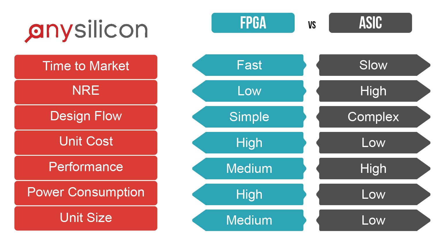
Time to Market:
With regards to the measure of time it takes to plan and foster FPGAs versus ASICs, FPGAs are by and large simpler and faster to deliver as they don’t need layout/masks and can be reprogrammed in the field on a case by case basis, so there is to a lesser extent a need to perform testing and verification processes like that of ASICs.
ASIC design, however, is more complicated, often requiring custom design and a complex design flow. Moreover, because of the intricacies and customizations, it can require a higher expectation to learn and adapt, stretching the time to market.
Ventures worried about an ideal opportunity to showcase over all the other factors are ought to think about FPGAs first. Contingent upon the intricacy of the plan, an FPGA can require weeks or months to plan. A structured ASIC takes around six to nine months, relying upon complexity. A cell-based ASIC requires somewhere close to 18 to two years.
NRE:
NRE represents Non-Recurring Engineering costs. As you can envision, with the words recurring and costs, each business is concerned when they hear those two words in a similar sentence. Thus, any reasonable person would agree that this is a fundamental primary consideration. Additionally, on account of ASIC, this is incredibly high, though, with FPGA, it is almost non-existent.
Be that as it may, in the grand scheme, the total costs get lower and lower the more massive the quantity you need in terms of ASIC. Besides, FPGA can set you back since its unit costs are higher per unit than ASIC.
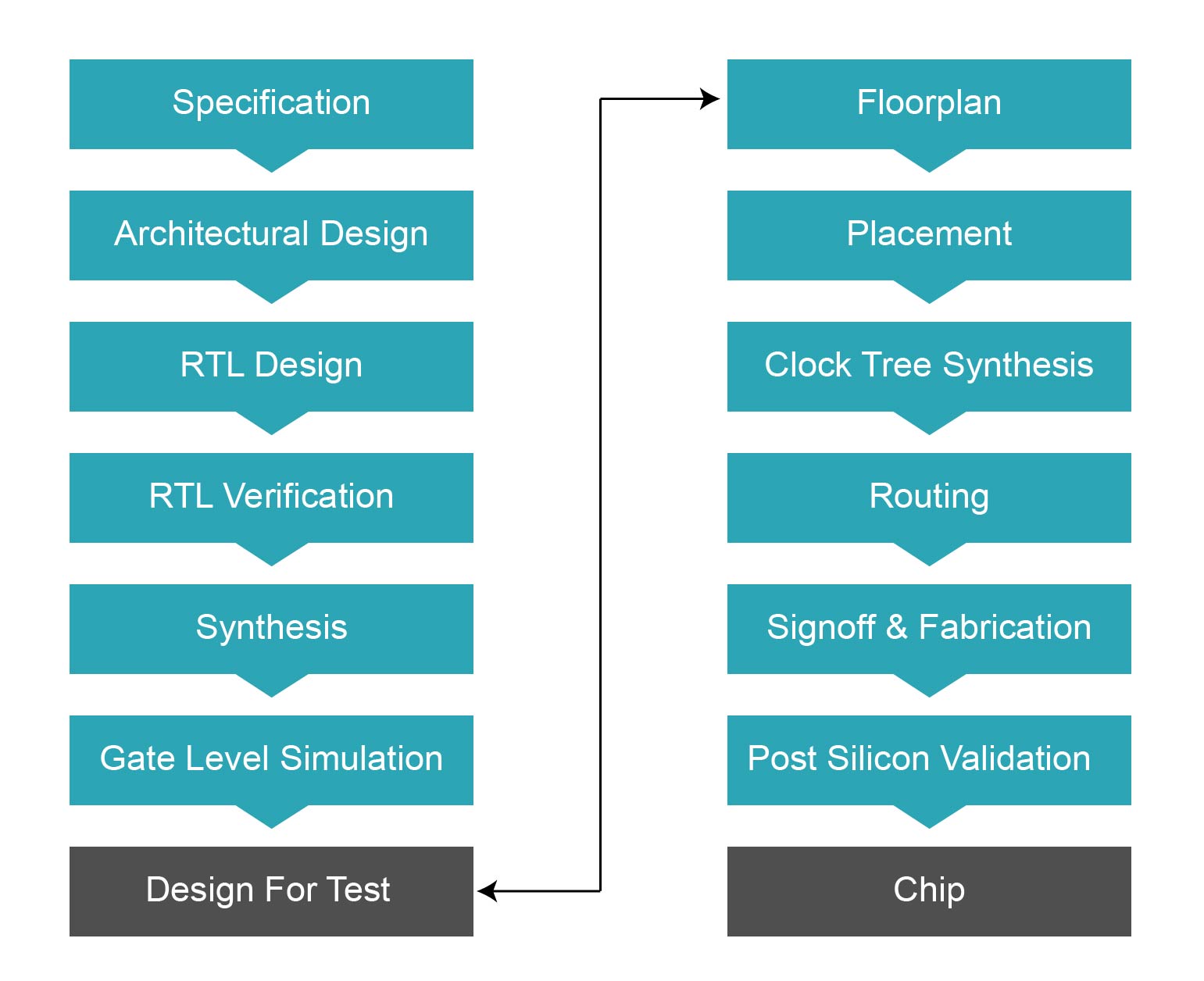
Design Flow:
Every Engineer and PCB designer favors a more difficulty-free and simplistic design process. Since what you do is mind-boggling, it doesn’t imply that you need to muddle the actual interaction. ASICs have a significantly more intricate and tedious design flow contrasted with FPGAs. Since ASICs are not reprogrammable, designers need to perform different processes, including design conceptualization, chip optimization, logical/physical implementation, design validation, and verification.
For FPGAs, such a design flow isn’t required. Since their function can be changed after fabrication, designs can take out the mind-boggling planning, place and route, and timing analysis.
FPGA Flow

ASIC Flow
Unit Cost:
Even though ASICs have a high NRE cost, the unit cost per chip is somewhat low, making it ideal for high-volume, large-scale manufacturing. Then again, FPGAs have a high unit cost, so this sort of chip isn’t appropriate for large-scale manufacturing. It is anyway thought to be financially savvy whenever created in more modest quantities.
Performance and Efficiency:
As far as performance, ASICs outflank FPGAs just barely, principally because of lower power utilization and the different potential functionalities that you can layer onto a single chip. Additionally, FPGA has a more rigid internal structure. At the same time, with an ASIC, you can design it to dominate in power utilization or speed. FPGAs require more power to perform comparable functions as ASICs.
Power Consumption:
Because ASICs are intended for a dedicated purpose, it offers better and speed contrasted performance than FPGAs. ASICs are likewise substantially more power-efficient than FPGAs because of their capacity to control and improve power utilization levels. Particularly with electronic gadgets that are battery worked. FPGAs require more power to perform comparative functions as ASICs.
Unit Size:
As far as size, it involves physical science. With an ASIC, its design is intended for one functionality; in this manner, it comprises precisely the number of gates needed for the ideal application. However, with FPGA’s multifunctionality, a single unit will be fundamentally bigger given its internal structure and a particular size that you can’t change.
Operating Frequency:
FPGAs have limited operating frequencies, the factor at the detriment of which we get the capability to reconfigure the chip. ASICs tend to have the ability to run at higher frequencies as compared to FPGAs at the same node, inferable from the fact that they have been designed to serve one function only and cannot be configured to accomplish something else.
Barriers to Entry:
Barriers to entry allude to the difficulty in acquiring these technologies and the forthright cost associated with them. Concerning ASICs, the barrier to entry is pretty high considering the high upfront NRE costs, the intricacy of operations, and other necessary ventures associated with it.
Reports show that ASIC development can range into the millions. In contrast, with FPGA, you can start development with less than a few grand (<$5000), making it the easier route to take in terms of capital speculation.
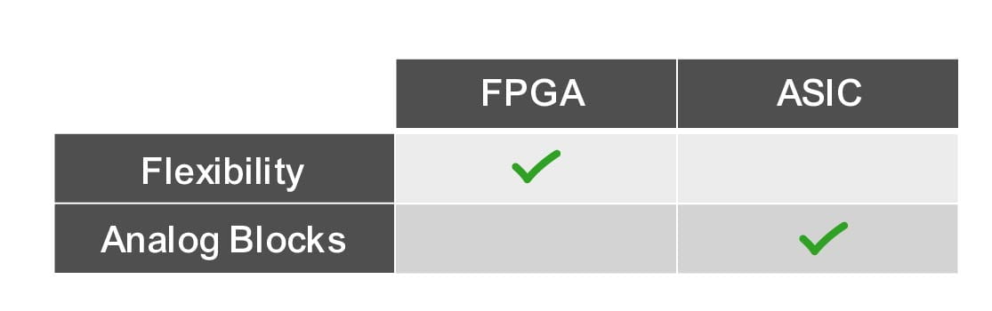
Configuration/Flexibility:
In general, the most evident distinction between FPGA and ASIC is programmability. Subsequently, the apparent result here is FPGA offers more choices as far as adaptability is concerned. FPGAs are not only flexible, but they also provide “hot-swappable” functionality that allows modification even while in use, a feature that makes it a popular choice among individuals and fields looking for high velocity, accelerated computing, such as in data centers
Analog Designs:
While FPGAs are reconfigurable, we can’t utilize them to make analog designs like ASICs. They can use analog hardware like ADC, RF blocks (Bluetooth, WiFi), and more to work with the analog design.
FPGA And ASIC Pricing
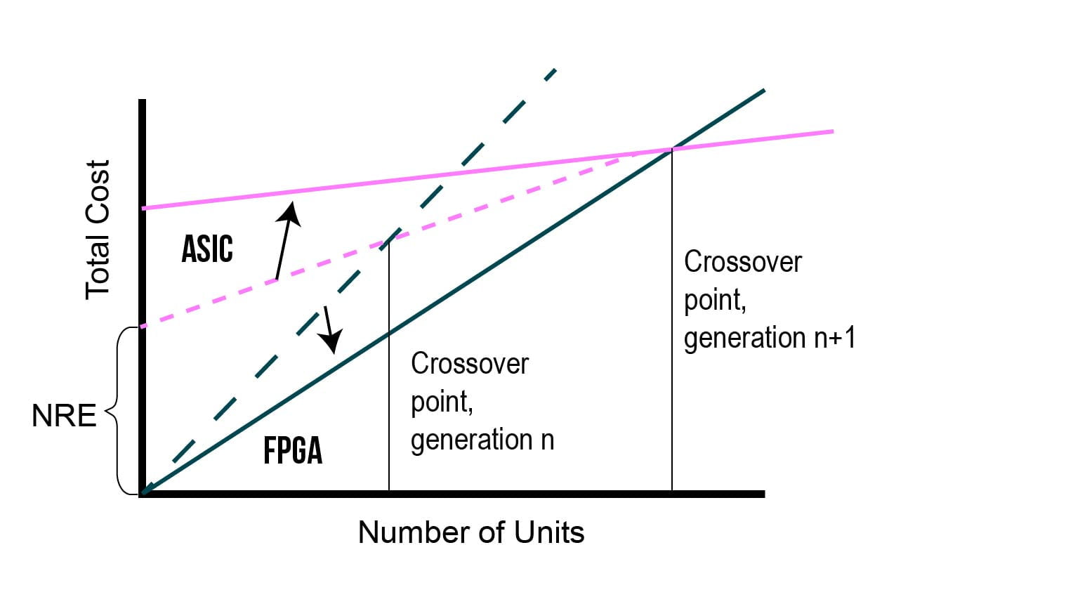
FPGA versus ASIC Crossover Point
The chart shows total expense versus the number of units. The inconvenience of the FPGA per-unit cost premium over ASIC lessened over the long run as NRE costs turned into a more significant part of the total cost of ownership of Application-Specific.
ASICs have exceptionally high Non-Recurring Engineering (NRE costs) up in millions. However, the actual per die cost could be in pennies. On account of FPGAs, there is no NRE cost. You pay for the genuine FPGA IC, and for the most part, get free software for that FPGA (up as far as possible). In this way, the total expense for ASICs begins extremely high inferable from the NRE cost;
however, its slope is flatter. That is, prototyping ASICs in small quantities is exorbitant. Yet, in huge volumes, the cost per volume turns out to be exceptionally more minor. On account of FPGAs, the IC cost is significantly higher, so in huge volumes, it turns out to be exorbitant in contrast with ASICs.
Here is the breakdown of ASIC cost parts:
- ASIC EDA tools and training
- Cost of designing
- DFT cost
- Cost of simulating
- ASIC Masks Cost
- Wafer Cost
- Wafer Processing
- Die Utilization
- Yield & Manufacturing Loss
- Packaging
FPGA vs ASIC Comparison summary

In contrast with the above list, the FPGA cost is just for the IC to pay off the rack..
You got Questions?
No Worries. We got you covered.
Related Post: FPGAs for Data Center Acceleration
FPGA FAQ’S
What is FPGA Mining?
FPGA mining is a highly effective and quick way of mining, contrasted with GPU mining and outflanks CPU mining. FPGAs regularly burn through small amounts of power with somewhat high hash ratings, making them more feasible and practical than GPU mining.
Can FPGA mine Bitcoin or Ethereum?
Indeed, it can. Yet, for Bitcoin, ASIC is now there, so it would make no sense for FPGA to contend with ASIC because ASIC would be much faster than FPGA. For Ethereum, ETH PoW calculation (Ethash) is memory escalated (requires a lot of memory).
FPGA isn’t appropriate because FPGA is core intensive; FPGA hashing speed would be around GPU. Be that as it may, FPGA with HBM can mine Ethereum quicker than GPU because HBM permits the accelerators to perform memory-bound compute tasks a lot faster than existing technology while burning through substantially less power than external DRAM.
How to cool your FPGA?
The following are the ways to cool the FPGA-
What are the different modes of programming the FPGA?
The different ways of programming the FPGA are –
- SRAM via JTAG or programmable cable
- Flash
- USB and SD-Card
What is a constraint file, and why do we use it?
A constraint file is required to make the design as per your requirements, like sending signals to particular pins of FPGA, defining clocks, setting false or multicycle paths.
Name some FPGA manufacturing companies.
- Xilinx (~50%)
- Altera (~40%)
- Lattice Semiconductor
- Microsemi(Actel)
- QuickLogic
What is the difference between ‘Hard Processor Core’ and ‘Soft Processor Core’?
By and large, FPGA is categorized in the following two ways in terms of design.
- Hard Processor Core – Some FPGA parts have fixed blocks like processor core and some typical standard IPs. There are few spaces available for other logic implementation.
- Capable of work on high speed due to better optimization.
- But have a fixed configuration and can not be altered.
- Soft Processor Core – Full FPGA can be utilized for logic. Users need to implement a soft processor core if required.
- It can be easily modified and have more logic
- But limited in terms of speed of the fabric
How does FPGA provide substantial benefits to enterprises?
As client request continues to change, manufacturers need to change or redesign their products to remain relevant. FPGAs are intended to give the required flexibility and make changes to the product functionalities anytime, even after deployment at the clients’ end.
The reception of FPGAs has been driven by the idea of consolidating the best features of ASICs and processor-based frameworks. FPGAs can be advantageous across different industries, given their features such as parallel processing, simple design cycle, adaptability, reusability, and quicker time-to-market.
ASIC FAQ’S
What is the development time from specification to ASIC prototypes?
ASIC design, including production silicon for cost decrease programs or scaling down, is accessible in 12-22 weeks. Analog ASIC prototypes can be finished in just two months relying upon the chip plan and intricacy. ASICs for new product advancement, where the performance and specification of the ASIC are dependent upon changes, take somewhere in the range of 18 and 28 weeks.
Do we need to partition our system-level schematics for ASIC integration before STA can provide us with a quote?
It very well may be helpful to however isn’t required. Our application engineers have a broad foundation in system design. They are persistently keeping up with knowledge of the size/valuing issues of discrete components.
What level of ASIC design expertise should we have to ensure a successful project?
The Customer ought to have a point-by-point familiarity with the system-level objectives and the working environment of the target product. No ASIC design proficiency is required.
What level of assistance is provided by STA during the prototype evaluation stage?
Ordinarily, we will evaluate prototypes for detailed conformance before they are shipped off to the client. When the timing of the evaluation is critical, a full assessment stage for the ASIC can be given.
Can the production schedule be expedited?
Indeed, now and again, tested parts can be conveyed in just fourteen days. Assisted timetables are accessible on a restricted premise.
How can we be sure that all production parts meet specifications?
The client should approve test flow and test limits before the beginning of production. Test parts tested by the production test program are provided for accreditation. At production, 100% of the wafers and 100% of packaged parts are tried for compliance.
What are the open-source tools being often used in ASIC Design?
- For Simulations- Xilinx Vivado, Mentor’s ModelSim.
- For Logic Synthesis- Yosys
- For Floor Planning, Placement, and CTS- Graywolf
- For Routing- Qrouter
- For STA- Open Timer
What is mixed-signal ASIC Design?
Mixed-signal ASIC design implements analog and digital circuits on a single semiconductor integrated circuit, which shares a standard power supply. This integrated circuit is viewed as an experimental stage for building savvy electronic applications.
What is Clock Gating?
The dynamic power associated with any circuit is related to switching activity and the total capacitive load. In digital VLSI designs, the most frequently switching element are clock elements (buffers and other gates used to transport clock signals to all the synchronous elements in the design).
In some of the designs, clock switching power may be contributing as high as 50% of the total power. Power being a very critical aspect, we need to make efforts to reduce this. Any measure that can be made to save the clock elements toggling can help in reducing the total power by a significant amount.
Clock gating is one of the techniques used to save the dynamic power of clock elements in the design. Clock gating is a popular technique used in many synchronous circuits for reducing dynamic power dissipation by removing the clock signal when the circuit is not in use. Clock gating saves power by pruning the clock tree at the cost of adding more logic to a circuit.
What Is Stuck-at Fault?
A Stuck-at fault is a particular fault model used by fault simulators and Automatic test pattern generation (ATPG) tools to mimic a manufacturing defect within an integrated circuit. Individual signals and pins are assumed to be stuck at Logical’ 1′, ‘0’, and ‘X.’
For example; an output is tied to a logical ‘1’ state during test generation to assure that a manufacturing defect with that type of behavior can be found with a specific test pattern. Likewise, the output could be tied to a logical 0 to model the behavior of a defective circuit that cannot switch its output pin.
Conclusion
FPGA or ASIC- What to Choose and When ? Still Confused?
On the off chance that you are an interloper in the VLSI world, FPGAs and Simulation Software are what you should go for. Likewise, the adaptability in the design of FPGAs makes it reasonable for applications and devices that need to be changed and often overhauled rather than ASICs appropriate for more long-lasting applications.
This component likewise settles on FPGA as the best decision for prototyping purposes. The circuit can be altered if there is a mistake or improvement, something impossible on an ASIC as it is permanent. That is the reason FPGAs are often used to prototype ASICs before they are made.
Then again, the last ought to be the go-to decision for large volume productions in case configurability is an immaterial factor.
If your design is advanced and remarkable with exceptionally explicit prerequisites (as far as cost, power, speed, and so on), then, at that point, you have no choice but to go with the ASIC route. Any other way, FPGAs can oblige most utilization cases, particularly when you need reconfigurable equipment.
The contention among FPGA and ASIC can be decided by your design type (analog or digital), configuration requirements, and budget. Despite the decision, the most important consideration ought to be your design needs. If you are as yet going back and forth, try simulation first.
If you would profit from utilizing FPGAs in your following product yet you’re uncertain where to begin; Logic Fruit Technologies can help.
We here at Logic Fruit are well equipped to make the fundamental compromises to optimize time to market, power, performance, cost, and unwavering quality of your product. We offer design services ranging from digital protocols to FPGA acceleration on data centers for real-time data processing.
To ultimately capitalize on the advantages of utilizing FPGAs, you need to band together with the right plan and creation group that can assist you with understanding your vision. Logic Fruit Technologies leverages expert designing and venture the executives’ abilities to help with each level of the design process.


![Advanced Driver Assistance System [ADAS] Everything You Needs to Know](https://www.logic-fruit.com/wp-content/uploads/2022/10/Advanced-driver-assistance-systems-Thumbnail.jpg)