
Field-Programmable Gate Arrays (FPGAs) are becoming an interesting alternative for next-generation High-Performance Computing (HPC) systems, with changeable fabrics delivering increased performance over time.
However, the optimisation process of FPGA designs should be abstracted to a higher level to gain traction among traditional Von Neumann systems.
Overall system performance, power consumption, thermal performance, and design cycle durations can all benefit from properly arranging device orientation on the board and allocating signals to appropriate pins.
You may optimize data flow across the device by visualizing how the device interacts physically and conceptually with the printed circuit board (PCB).
In this blog, I will share the standards incorporated in analysing and optimizing the FPGA requirements and shed some light on how a designer can improve performance with device selection. To understand and know more about the trends in FPGA technology and market expansion, you can read here.
PCB Layout selection
- The device’s orientation on the PCB should be established first. Take into account the position of fixed PCB components and internal device resources. Shorter PCB trace lengths and fewer PCB vias can be achieved by positioning the GT interfaces on the device package as close as possible to the components with which they interface on the PCB. A schematic of the PCB with the essential interfaces may frequently aid in determining the optimal orientation for the device on the PCB, as well as the placement of PCB components. After that, you may plan the rest of the device’s I/O interface.
- Memory interfaces, for example, can benefit from having relatively short and direct connections to the PCB components with which they interact. If at all feasible, the length of these PCB traces must be matched, and PCB vias must be avoided. To keep the connections short and avoid routing out of the vast matrix of BGA pins, the package pins closest to the device’s edge are chosen in these instances. At this point, the Vivado ® IDE’s I/O Planning view layout comes in handy for visualizing I/O connectivity concerning actual device dimensions, with top-side and bottom-side views.
Power Distribution
- When developing a power distribution system (PDS) for a device, board designers are presented with a unique challenge. Most other big, dense integrated circuits (such as huge microprocessors) have extremely precise needs for bypass capacitors. Because these devices’ hardened silicon architecture is only meant to perform particular functions, their power supply demands are fixed and generally vary within a set range.
- As a result, you must understand the design’s power needs, which you can do by doing a power estimation with the Xilinx Power Estimator (XPE). Before estimating power, read the PCB Design Guide for your device to fully understand the PDS location and general decoupling needs.
- The following are important elements to consider while designing a PDS:
- Using power estimate to choose the correct voltage regulators to satisfy the noise and current requirements.
- Configuring the XADC power supply (Vrefp and Vrefn pins).
- Performing a simulation of a power distribution network (PDN).
Considerations for a Thermal Solution
When evaluating the power of a system, it’s crucial to know how efficient the thermal solution is. As the junction temperature drops, the static power of a design reduces.
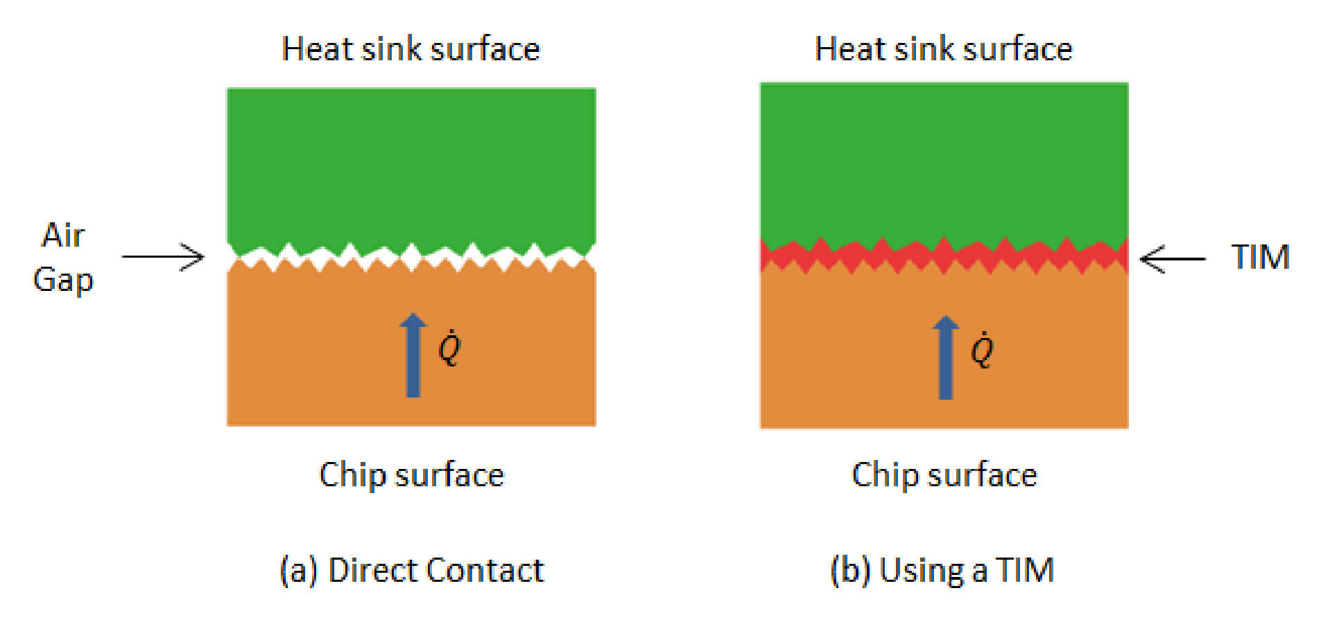
If your device supports lidless packing, as Xilinx advises, use it. Lidless packaging provides a more effective thermal solution by eliminating the thermal interface material (TIM) layer and allowing direct contact with the heat source.
The chip’s backside is exposed in the lidless arrangement, allowing direct contact between the chip and the heat sink, which improves the chip’s overall thermal performance.
While lidless packages have greater thermal performance, flat- and full-lidded packages are more convenient to handle since they include a lid that protects the die while also distributing heat.
Design Considerations
Every electrical equipment we use today is subject to electromagnetic interference (EMI). When you turn on your radio and TV at the same time, the TV signal will interfere with the radio signal and vice versa, causing a noisy nuisance.
The PCB should be built with the quickest signal interface to the device in mind. Trace geometry, vias, loss, and crosstalk are all very sensitive to these high-speed signals. When it comes to multi-layer PCBs, these factors become much more important.
Perform a signal integrity simulation for high-speed connections. To achieve the needed performance, a board redesign with better PCB material or changed trace shapes may be required.
Device Power Aspects
A gadget requires multiple power supplies, which must be delivered in a certain order. Consider using power monitoring or sequencing circuitry to ensure that the device, as well as any other active components on the board, receive the proper power-on sequence.
To regulate the power and reset procedure in more sophisticated settings, a microcontroller or a system and power management buses such as SMBus or PMBus may be used.
Power Types
- Power-On: The transient spike current that happens when power is first introduced to the device is known as power-on power. This current varies per voltage supply and is determined by the device’s design, the power supply source’s capacity to ramp up to the nominal voltage, and the device’s working circumstances, such as temperature and supply sequencing. When the correct power-on sequencing criteria are followed, spike currents are not an issue in contemporary device designs.
- Startup power: Startup power is the amount of energy necessary to set up and configure a device. Thermal dissipation isn’t a concern with this power because it’s created in such a short amount of time. However, current requirements must be met. In most cases, the active current of an operating design will be higher, therefore no changes are necessary. However, a higher current demand during this time may be required for lower-power systems with a low active current. This need may be deduced using XPE. When the Process is set to Maximum, the current requirement for each voltage rail is set to the higher of the running current or the starting current. If the starting current is higher, XPE will display the current value in blue.
- Static Power: The power supplied while the device is equipped with your design and no activity is applied outside or created internally is known as design static power (also known as standby power). The minimal continuous power that the supplies must deliver while the design is operational is referred to as static power. The static current ICC, which flows independent of gate switching (transistor is ON “biased” or OFF “unbiased”), is proportional to the FPGA static power.
- Dynamic power: The power required when the device is executing your application and moving between High and Low logic values when clocks and data paths change between High and Low logic values is referred to as dynamic power. The average switching activity of device circuits over time is used to compute dynamic power.
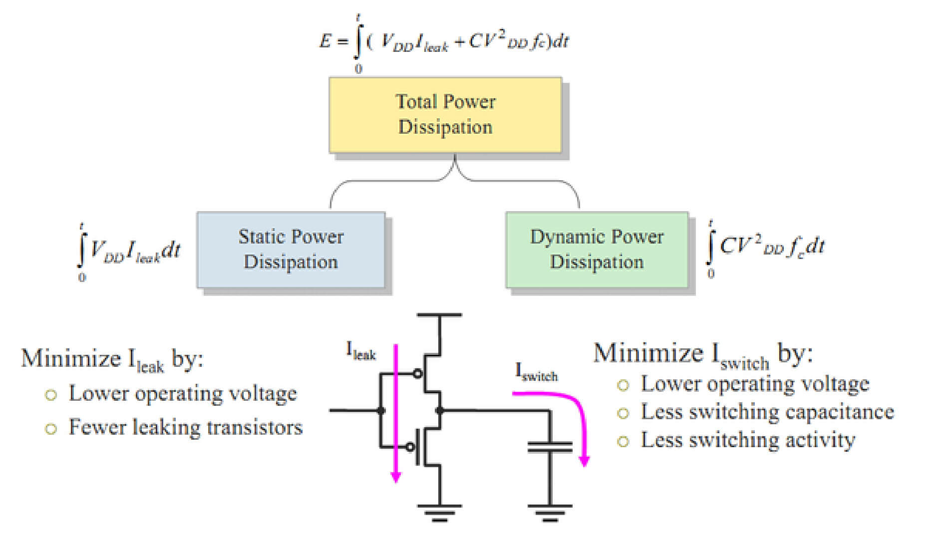
Total power is the sum of static and dynamic power. Slowing down the design (reducing clock speeds), lowering voltages, or reducing design activity are all ways to preserve dynamic power.
Another significant component of conserving power is reducing capacitances in the design, which can usually be done by efficient implementation or process tuning.
Pin Assignment
Good pinout selection leads to more efficient design logic placement, shorter pathways, lower power consumption, and better performance. Because a spread-out pinout might allow linked signals to cover greater distances, good pinout selection is especially critical for large devices.
Interactive design planning and pin selection are made easier using Xilinx tools. These tools are only as good as the data you give them with.
Pinout attempts can be aided by tools like the Vivado I/O Planner. These tools can illustrate I/O location graphically, demonstrate connections between clocks and I/O components, and give DRCs for pin selection analysis.
You must supply as much information about the I/O features and topologies as feasible for the tools to operate properly. The electrical properties of the I/O must be specified, including the I/O standard, drive, slew, and direction.
Choosing a Pinout
- The same interface data, address, and control pins should all be grouped in the same bank. If you can’t fit all of these items into the same bank, put them in nearby banks.
- Clocking, enables, resets, and strobes are the interface control signals that should be placed in the center of the data buses they regulate.
- Design-wide control signals with a high fanout should be directed towards the device’s core.
Memory Interfaces
When utilizing any Memory IP, additional I/O pin designing procedures are necessary. After customizing the IP, assign the top-level IP ports to physical package pins in the Vivado IDE’s elaborated or synthesized design.
For easy identification and assignment, all of the ports associated with each Memory IP are grouped into an I/O Port Interface. To help you assign Memory I/O pin groups to byte lanes on the actual device pins, a Memory Bank/Byte Planner is included.
When allocating memory interfaces, be cautious and attempt to keep congestion to a minimum, especially on devices with a center I/O column. When memory interfaces are grouped, routing bottlenecks might form across the device.

Gigabit Transceivers (GTs)
The pinout requirements for gigabit transceivers (GTs) are as follows:
- Reference clocks are shared.
- Within a quad, PLLs are shared.
- Hard blocks, such as PCIe, and their placement to transceivers.
- SLR boundary crossing in SSI technology devices.
Configuration
Configuration is the process of loading application-specific data into the device’s internal memory. The configuration data for Xilinx devices are volatile and must be reloaded every time the device is turned up because it is stored in CMOS Configuration Latches (CCLs).
When designing your board, think about the configuration aspects first, as this will make it easier to configure and debug afterward. The Configuration User Guide for each device family is the most comprehensive source of information on each of the different configuration modes and the trade-offs between pin count, performance, and cost.
Conclusion
Modern FPGAs have advanced technology as well as support for high computing rates, more networking options, high-security features, and high bandwidth.
Logic Fruit Technologies designs and develops a wide range of FPGA technology for a variety of applications, including Telecom, Defense & Aerospace, Testing & Measurement, Artificial Intelligence Semiconductor, and Image & Video Processing.
When designing for larger density FPGAs, techniques for attaining the best design performance are crucial. The instruments that allow these strategies must be as flexible as possible without sacrificing ease of use.
The timing model utilised during compilation is determined by assigning a specific device. To get accurate results and the best optimization, it’s crucial to pick the right speed grade. The number of resources used is determined by the device size and package.


![Advanced Driver Assistance System [ADAS] Everything You Needs to Know](https://www.logic-fruit.com/wp-content/uploads/2022/10/Advanced-driver-assistance-systems-Thumbnail.jpg)