Introduction
Field-Programmable Gate Arrays (FPGAs) lead modern digital design. They’re a flexible, lively replacement for typical integrated circuits.
They have a unique architecture made of interconnects and changeable logic blocks. This allows designers to make custom digital circuits using Hardware Description Languages (HDLs) like VHDL or Verilog.
The reasons why FPGAs shine in the fast-paced world of digital tech are, that they’re able to be reprogrammed, they power to process multiple tasks at once, and they ability to be customized. These factors make them an important part of digital technology.
This blog explores the broad applications and architecture of FPGA design, diving into an intricate field.
FPGAs are influencing how digital innovation will develop in the future by speeding up algorithms in high-performance computing and enabling quick prototyping during the development cycle.
Come along on a journey to learn about the FPGA architecture, FPGA design flow, and its applications, which give digital designers and engineers a valuable tool.
FPGA Design
FPGA Design: An FPGA is a programmable logic device with a matrix of reconfigurable gate array logic circuits. When an FPGA is configured, the internal circuitry is coupled in such a way that the software program is implemented in hardware.
Unlike processors, FPGAs process logic on dedicated hardware and do not have an operating system.
Different processing operations do not have to fight for the same resources because FPGAs are really parallel in nature. As a result, when extra processing is introduced, the performance of one section of the application is unaffected.
Intel, Xilinx, Lattice Semiconductor, and Microchip Technology are among the major FPGA manufacturers.
Additionally, numerous control loops can execute at different rates on a single FPGA device.
Critical interlock logic can be enforced by FPGA-based control systems, and they can be built to avoid I/O forcing by an operator.
Unlike hard-wired printed circuit board (PCB) designs with set hardware resources, FPGA-based systems can actually rearrange their internal circuitry to allow reconfiguration once the control system has been deployed to the field.
Dedicated hardware circuitry’s performance and dependability are delivered by FPGA devices.
Learn More About: PCIe GEN6 Controller IP
FPGA Design Flow
A number of distinct steps or phases make up the FPGA design flow, including design entry, synthesis, implementation, and device programming. We’ll go into great detail about each of these stages.
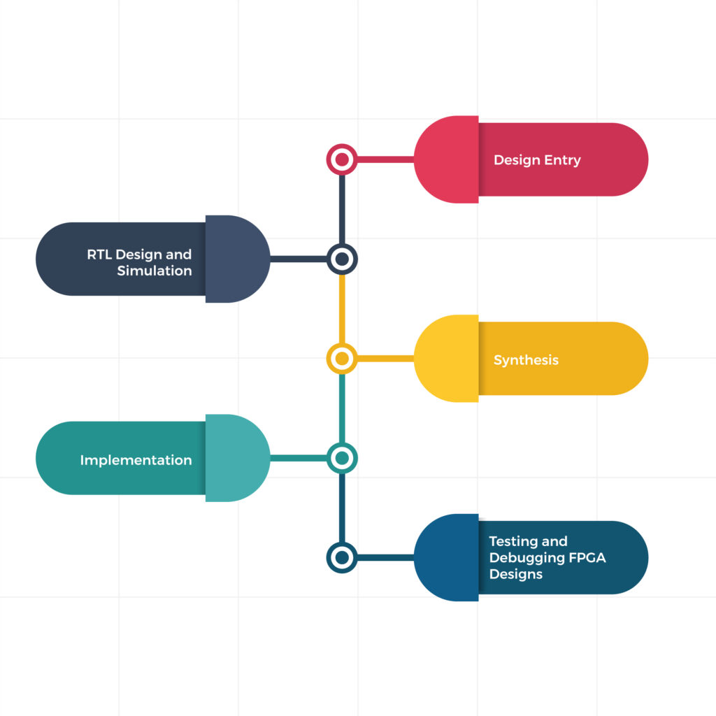
Design Entry
Depending on your FPGA design and preference, you can enter designs using a variety of methods, such as schematics through Hardware Description Language (HDL) or you can use a combination of the two and a best-of-both-worlds approach using tools that can convert HDL into schematics and vice versa.
Generally speaking, HDL is a better option for designs involving more complex systems because it is a faster, language-based process that eliminates the need to design in lower-level hardware. However, schematics are a good option for hardware designers because they provide more system visibility.
A state-machines-based strategy is another option, but it is currently underutilized and very restricted. It works well for designers who see their work as a progression of states.
Every strategy has advantages as well as disadvantages. Even though a schematic-based approach is simpler to read and understand, it is typically limited to smaller projects. Alternatively, HDL-based approaches are currently the most popular design entry for FPGA designs because they are typically quick and simple to implement.
RTL Design and Simulation
A digital circuit’s RTL design is an intermediate representation that concentrates on the data flow between registers and the operations carried out on that data. Before proceeding to the synthesis and implementation phases, the functionality and performance of the design are confirmed via RTL simulation.
The RTL simulation tools ModelSim, XSIM, and VCS are commonly used. Functional and timing simulations, made possible by these tools, aid in the early detection and correction of design flaws and performance bottlenecks.
Synthesis
This step involves translating the design from code, which has been entered, into an actual circuit with components like gates, flip flops, and multipliers, among others. In essence, your input HDL is transformed into a netlist that enumerates the logic components and interconnects required in the particular hierarchy for your project.
As soon as you feed in your HDL-based design, the procedure starts with a syntax check. Then, it is made faster to implement by reducing the amount of logic, getting rid of unnecessary logic, and shrinking the design’s overall size. The final stage involves mapping out the technology by integrating the design with the logic, calculating the corresponding time, and creating the design netlists, which are then saved.
Specialized synthesis tools are used for FPGA synthesis. FPGA synthesis tools are developed, marketed, and sold by EDA companies Cadence, Synopsys, and Mentor Graphics.
Implementation
This stage, which consists of three steps translation map, place & route—will determine the layout of your design. The FPGA vendors supply the tools used in this step because they are the experts at converting a synthesized netlist into an FPGA.
The tools’ initial step is to compile all user-specified constraints along with the netlist files. These limitations may relate to the pin assignments and locations, timing specifications like the maximum delay, or the clock’s input period.
The implementation is then mapped out by the tool by contrasting the resources that are actually available on the FPGA that are being used with the resource requirements that are specified in the files. The circuit is separated into sub-blocks, or logic blocks, or elements. Your entire design is therefore “mapped out” into the FPGA and put into designated logic blocks.
The next stage involves connecting and routing each signal between each logic block and each IO block in line with the user-specified constraints.
Testing and Debugging FPGA Designs:
In order to make sure that the FPGA design works as intended and satisfies performance standards, testing and debugging are essential stages in the process. Typical testing techniques consist of
Simulation: Using simulation tools to test the design in a virtual environment, allowing for faster and more controlled testing.
In-circuit testing: Testing the FPGA design on the testbench or target hardware, often using a logic analyzer or an oscilloscope to monitor signals and identify issues.
Debugging FPGA designs entails locating and resolving problems with performance, functionality, and resource usage. Among the best debugging techniques are:
To make code easier to read, use names for variables and signals that are descriptive. Using a modular design strategy to divide the design into more manageable, smaller parts. Utilizing in-circuit testing and simulation tools to find and isolate problems.
High-quality FPGA designs that satisfy the demands of particular applications can be produced by designers by adhering to the FPGA design flow and using best practices for testing and debugging.
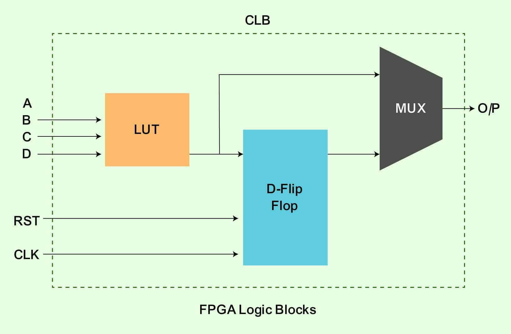
Configurable Logic Blocks (CLBs)
Three key components make up the CLBs: the multiplexer, flipflop, and LUT in FPGA. A multiplexer is used to choose between combinational and sequential logic for the data output, with the LUT serving as the main component capable of implementing the logical function.
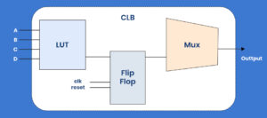
Look-Up Tables (LUTs) and Flip-Flops
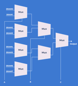
The LUT, which forms the basis of an FPGA architecture, is among its most crucial components. LUT is made to work with any Boolean formula. Multiplexers and SRAM cells that store the outputs based on the select lines are located inside the LUT.
It takes two thousand SRAM bits and a two thousand:1 multiplexer to implement a k-input LUT (k-LUT), which is a LUT that can implement any function of k inputs. The image below illustrates a 3-LUT, which is made up of an 8:1 multiplexer implemented as a tree of 2:1 multiplexers and 8 bits of SRAM.
By allocating the proper value to each of the three inputs (A, B, and C), the 3-LUT can implement any function that requires three inputs.
Clock Management
As we’ve seen, we have two choices for implementing logic on FPGA: sequential logic or combinational logic. The key component of the design is clock resources, which must be jitter-free, low power, highly precise duty cycle, and efficient in order for sequential logic to function. To generate the necessary frequency clock signals, the FPGAs have integrated hardware for phase lock loop (PLL) and delay lock loop (DLL).
FPGA Architecture
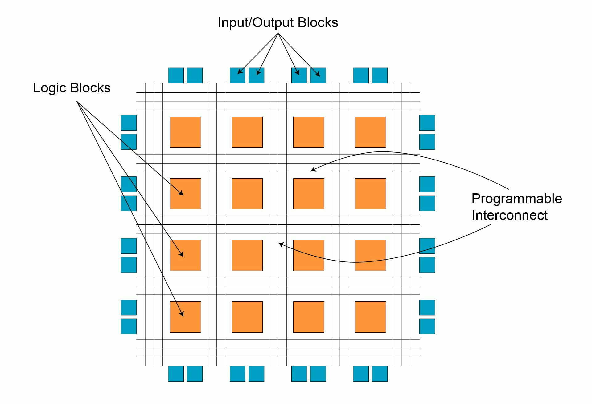
Block RAMs, DSP Slices, PCI Express compatibility, and programmable fabric are all part of FPGAs’ heterogeneous computation platforms. Because all of these compute resources can be accessed at the same time, they enable parallelism and pipelining of applications throughout the platform. An FPGA’s basic structure consists of logic units, programmable interconnects, and memory. The placement of these blocks is unique to each manufacturer.
FPGAs can be classified into three groups based on their internal block arrangement:
Symmetrical arrays
The logic elements (called CLBs) are placed in rows and columns of a matrix, with connections built out between them. I/O blocks surround this symmetrical matrix, connecting it to the outside world. A pair of programmable flip-flops and an n-input Lookup table make up each CLB.
Functions such as tristate control and output transition speed are likewise controlled by I/O blocks. Interconnects are used to create a routing path. When compared to general-purpose interconnect, direct interconnects between neighboring logic elements have a shorter delay.
Row-based architecture
Alternating rows of logic modules and customizable connection tracks make up a row-based design. The input-output blocks are located on the row’s periphery. Vertical interconnects can connect one row to neighboring rows.
Logic modules can be combined in a variety of ways. Combinatorial modules are made up entirely of combinational parts. Sequential modules include both combinational and flip-flop features. Complex combinatorial-sequential functions can be implemented with this sequential module. Anti-fuse components are used to connect the smaller pieces of the routing rails.
Hierarchical PLDs
This architecture is organized hierarchically, with just logic blocks and interconnects at the top level. There are a number of logic modules in each logic block. Each logic module includes both combinatorial and sequential functional features.
The programmed memory controls each of these functioning parts. Programmable interconnect arrays are used to communicate between logic blocks. This system of logic blocks and interconnects is surrounded by input-output utilized blocks.
Internal Structure of an FPGA
Each FPGA includes three important features that can be found at the heart of modern-day FPGA architecture:
Logic Blocks
An FPGA’s logic blocks can be designed to provide functionality as simple as that of a transistor or as complicated as that of a microprocessor. It may be used to implement a variety of sequential and combinational logic functions.
Modern FPGAs are made up of a variety of distinct blocks, such as dedicated memory blocks and multiplexers. To control the precise function of each piece, configuration memory is used across the logic blocks. Any of the following can be used to implement logic blocks in an FPGA:
- Transistor pairs
- combinational gates like basic NAND gates or XOR gates
- n-input Lookup tables
- Multiplexers
- Wide fan-in And-OR structure
Routing
In FPGAs, routing is made up of wire segments of variable lengths that are joined by electrically programmable switches. The length and number of wire segments utilized for routing determine the density of logic blocks used in an FPGA.
The number of connecting segments utilized is often a compromise between the density of logic blocks employed and the amount of space taken up by routing. To complete a user-defined design unit, programmable routing connects logic blocks and input/output blocks. Multiplexers, pass transistors, and tri-state buffers make up this circuit. In a logic cluster, pass transistors and multiplexers are utilized to connect the logic units.
I/O blocks
An input/output (I/O) block is a type of input/output device that can be used for both input and output. Edge-triggered D flip flops are used in both the input and output channels. The goal of the I/O blocks is to give a user interface from the outside world to the internal architecture of the FPGA. These cells take up a lot of space on the FPGA.
The design of I/O programmable blocks is very difficult due to the large variances in supply and reference voltages. In I/O architecture design, the standard selection is critical. Supporting a high number of standards might increase the size required for I/O cells on a silicon device.
Applications
Field-Programmable Gate Arrays (FPGAs) are versatile integrated circuits that can be configured and reconfigured to implement a wide range of digital circuits and functions. Here are some common applications of FPGAs:

Aerospace & Defense
FPGAs, or field programmable gate arrays, are important in the aerospace and defense industries. Signal processing, radar systems, avionics, cybersecurity, UAVs, electronic warfare, testing, and space exploration are the main applications of FPGA in aerospace and defense.
Additionally, it offers a high-performance, flexible, and adaptive solution that guarantees systems maintain their relevance through upgradability without requiring total hardware overhauls.
Automotive
Advances in safety, performance, and connectivity in automotive technology are made possible by FPGAs. They facilitate sensor fusion and provide critical processing for autonomous driving in addition to providing real-time processing for ADAS.
FPGAs support cybersecurity, functional safety, and power efficiency in addition to infotainment and V2X communication customization. They will be crucial in influencing the development of automotive systems in the future due to their versatility and reconfigurability.
Data Center
Field-Programmable Gate Arrays (FPGAs) are becoming more and more popular in data centers because of their energy efficiency, customization options, and capacity for parallel processing. FPGAs are used in accelerated computing, network function virtualization, and enhanced security through accelerated cryptography.
They also offer dynamic reconfiguration and lower latency. Cost considerations and complex programming are challenges. It is anticipated that FPGAs’ role in data centers will grow as technology advances and programming tools advance, offering enhanced performance, energy efficiency, and innovative data processing.
Medical
Biomedical images produced by PET procedures, CT scans, X-rays, three-dimensional imaging, and other techniques are increasingly being treated using FPGA design.
The benefits of frequency come from the fact that these medical vision systems increasingly need greater resolution and processing power, and many of them must be designed in real-time. Parallel processing and FPGA design are ideal for meeting these needs.
Video and Image Processing
FPGAs use parallel processing to handle data simultaneously, making them essential for processing images and videos. They are perfect for real-time applications like streaming and medical imaging because of their adaptable architecture, which maximizes performance and resource usage.
FPGAs speed up deep learning inference and are excellent at object recognition, video compression, and image enhancement. Their versatility includes a wide range of I/O and camera interfaces, which makes system integration easier.
Digital Signal Processing
Field-programmable gate arrays, or FPGAs, are essential to digital signal processing (DSP) because of their parallel processing capacity and reconfigurability. Real-time signal processing, image, and video processing, software-defined radio, speech and audio processing, sonar and radar systems, digital filters and transformations, and biomedical signal processing are examples of common applications.
FPGAs are indispensable in a variety of fields requiring high-performance and customizable signal manipulation because they excel in these areas by enabling real-time, parallelized execution of complex algorithms.
Wireless Communications
Wireless communications are undergoing a revolution thanks in large part to Field-Programmable Gate Arrays (FPGAs), which provide unmatched flexibility and adaptability.
Their reconfigurable nature makes it easier to quickly implement different communication standards, such as LTE and 5G, and their parallel processing capabilities improve throughput and processing speed in real-time. Baseband processing, MIMO systems, Software-Defined Radio, and cognitive radio applications are areas in which FPGAs thrive.
Conclusion
Field-programmable gate arrays, or FPGAs, are dynamic devices that allow for flexible hardware implementation thanks to their programmable logic blocks and configurable interconnects. Without the need for custom silicon, their architecture, which includes programmable elements and embedded components, enables flexible digital circuit design.
FPGAs are used in many different industries for a variety of tasks, including hardware acceleration and real-time signal processing. In conclusion, FPGAs are essential in the field of digital hardware design and a wide range of applications because they provide a powerful blend of performance and adaptability.