The digital interface frequently acts as a throughput limiter when data converter rates rise. The necessity to create a consistent procedure for serializing digital data from data converters and to minimize the number of connections between mixed-signal devices and processing elements like field-programmable gate arrays (FPGAs) gave rise to the JESD204 interface standard.
The B version of the standard, which is one of the most widely used and recognized by device developers, is one of its many revisions.
We will explore the JESD204B, its characteristics, advantages, applications, and more in this blog.
The Arrival of JESD204B
The standard’s second version, JESD204B, was published in July 2011. The addition of clauses to provide deterministic latency was one of the updated standard’s main elements.
Furthermore, the data rates that were supported were increased to 12.5 Gb/s and divided into various device speed grades.
The device clock should be used as the primary clock source instead of the frame clock, according to this edition of the standard.
The JESD204 standard does not include any mechanisms to guarantee predictable latency across the interface in its first two iterations.
The JESD204B revision addresses this problem by offering a way to guarantee that the latency should be predictable and repeatable both across connection resynchronization events and from power-up cycle to power-up cycle.
Key features of JESD204B
Delivering Performance
- By the JEDEC JESD204B specification
- Line speeds range from 1 Gbps to 12.5 Gbps, with a 25 Gbps extension possibility.
- supports lanes 1–24
- 1-96 converters are supported.
- HD mode compatible
- Performs user-friendly scrambling
- Creates the first series of lane alignment
- Generates alignment characters.
- Verifies link configuration data during the initial lane synchronization sequence using user-selected parameter values.
- 8b 10b encoding
- Verilog-oriented
- Data mapping and de mapping options
- Supports Subclasses on the 8b10b link layer (0, 1, and 2).
Interoperability
- Numerous data converters have been used to test the interoperability of JESD204B IP.
- Interoperability tests have been conducted between JESD204B IP and major SerDes PHY solution providers.
Easy to use
- A platform for demonstrating hardware is accessible.
- Regression and VIP test suites are offered.
- SerDes compatibility with several significant vendors
- Included is the basic test bench.
Silicon Agnostic
- Created in Verilog with an emphasis on FPGAs and ASICs
JESD204 High-Speed Interface
The JESD204B interface standard considerably reduces the number of digital IOs required, which eases board layout, while supporting the high bandwidth required to stay up with today’s top high-performance, high-speed, and multi-channel applications.
These days, very high-speed ADCs can be achieved with a few pins instead of a complex interface design utilizing many FPGA IO.
Without requiring extra pins, the JESD204B interface’s overall bandwidth can also be divided into numerous channels according to the needs of the application.
New terminology for JESD204B
The JESD204B protocol is the preferred interface for data transfer to FPGAs (or bespoke ASICs) when high-speed analog-to-digital converters (ADCs) approach the Giga sample-per-second (GSPS) level.
Wideband RF ADCs are required to collect RF spectrum at higher frequencies. A high-speed serial interface the JESD204B in this case is required with the move toward GSPS ADCs, which capture broader bandwidths and enable more customizable SDR (software-defined radio) platforms.
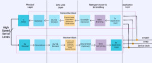
Recognizing that the JESD204B standard is a layered specification is crucial.
Every layer in the specification serves a specific purpose. The JESD204B link’s configuration and data mapping are made possible by the application layer.
Conversion samples to and from framed, non-scrambled octets are mapped by the transport layer.
To lessen EMI impacts by spreading the spectral peaks, the scrambling layers can take such octets and scramble or descramble them. Descrambling would take place in the receiver and scrambling in the transmitter.
The 10-bit characters are encoded from the optionally jumbled octets at the data link layer. Additionally, control character generation or detection for lane alignment monitoring and maintenance is carried out in this layer.
The serializer/deserializer, or SERDES, layer, which is part of the physical layer, is in charge of sending and receiving characters at line-rate speeds. The serializer, drivers, receivers, clock data recovery, etc. are all included in this layer.
The way these layers are arranged in the JESD204B specification is depicted in the graphic below.
A detailed look at each layer will help you better comprehend the specification by enabling you to see how the ADC samples are mapped to 8b/10b serialized words.
Simplified Data Flow Through JESD204B Layers
Application Layer
The application layer permits mapping sample data outside of the standard JESD204B specification, as well as unique user customizations.
This may make it possible to exploit the interface more effectively to achieve power savings and other advantages.
These specific configurations need to be set up on the transmitter (ADC) and receiver (FPGA). It’s critical to keep this in mind.
To ensure that data is transferred and understood accurately, the transmitter and receiver must be configured the same.
For ADCs that have to pass data in sample sizes that could differ from N’ (the number of transmitted bits per sample), setting up the application layer uniquely can be helpful.
This might make it possible to repack many samples in a way that lowers the lane rate and raises the link efficiency overall.
Transport Layer
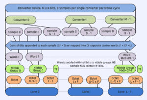
Next, look more closely at the JESD204B specification’s transport layer. To create nibble groups—typically on 4-bit boundaries the transport layer takes the ADC samples and adds information or padding.
These data come in the form of tail or control bits, which can offer more details about the data that was sent. Frames are created by the transport layer using these nibble groups.
Notably, the samples are sent as parallel data from the transport layer to the data link layer.
The width of the parallel data bus is determined by the framer architectures (single byte is 8 bits, dual byte is 16 bits, etc.) The serializer has yet to be reached in the data flow at this point.
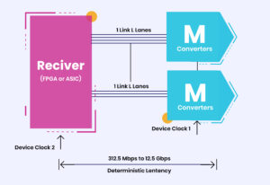
One ADC can be mapped to either a multi-lane link or a single-lane link. For GSPS ADCs used in wideband RF applications, where the sample rate requires the usage of many lanes to meet lane rate constraints, this configurability is quite helpful.
For M number of ADCs in the same device, multiple converters can also be mapped onto multiple lanes. The ADCs can be mapped to either a multi-lane link with L lanes or a single-lane link.
An ADC may require many lanes in specific situations. This is determined by a certain ADC’s lane rate maximum.
The highest lane rate for the 12-bit 2.5 GSPS AD9625, for instance, is 6.5 Gbps. That is, eight lanes in total are needed when N’ is equal to 16.
Occasionally, the system’s FPGA may place a limit on the lane rate. Cost may be one design parameter for clients utilizing GSPS ADCs in their RF applications.
It may be possible to reduce costs by using an FPGA with reduced lane rate capabilities. For instance, the maximum lane rate of the 14-bit 1.0 GSPS dual channel AD9680 is 12.5 Gbps.
The AD9680 can be set up to employ decimation to reduce the sample rate and, consequently, the lane rate. It has four output lanes. This reduces the pace of a certain lane and selects a bandwidth for a particular RF application.
Let’s return to the JESD204B specifications. The JESD204B word size is given by the N’ parameter. Four-bit nibbles make up the converter sample resolution. Three nibbles are present in a 12-bit converter, compared to four in a 14- and 16-bit converter.
It is possible to reduce the number of required lanes by 2 such that 6 lanes are needed to maintain a lane rate of less than 6.5 Gbps if N’ is set to 12 for the AD9625.
On 4-bit nibble boundaries, it is advised to map the conversion samples (S) into JESD204B words.
The ADC sample mapping into the serial lanes is depicted in the photos below. It has been parameterized to account for all possible scenarios that JESD204B can be used for.
The number of nibbles multiplied by four yields the N’ parameter. For converters that have resolutions between eight and sixteen bits, setting N’ to sixteen can be beneficial to both the transmitter and the receiver. This simplifies system design overall by enabling the use of the same transmitter and receiver for many converters.
According to the JESD204B standard, a non-complete nibble contains space for either control bits (CS) or tail bits. There must be a solution to the equation N’ = N + CS + T. Any control bits are added to each conversion sample after the LSB.
The number of octets sent to each frame, F can be found by multiplying the number of converters by the number of samples per frame, the JESD204B word size, and the maximum lane rate.
The equation F = (M x S x N’)/(8 x L) can be used to find this parameter. Refer to reference 1, which goes into further depth about the JESD204 link settings, for additional information.
Further details on the JESD204 standard are also available through a four-part webinar series, which starts with the transport layer.
Transport Layer ADC Sample Mapping
The connection configuration parameters that have been specified for a particular device are used by the transport layer to decide how to pack the data from the ADC.
During the Initial Lane Alignment Sequence, these parameters are sent from the ADC to the FPGA (ILAS).
To define the connection configuration parameters, these settings are configured using a Serial Port Interface (SPI), which sets register values on the FPGA and ADC.
For the receiver (FPGA) to confirm that the link configuration parameters were received accurately, a checksum is constructed from the parameters and communicated.
The parameters that are supplied via the link are solely used to confirm that the link parameters match, not to configure the receiver.
If a fault is found, the FPGA will report it via an interrupt, as specified in the JESD204B specification’s error reporting.
Implementing the JESD204B interface on an FPGA
Design Considerations
Several design concerns must be made when implementing JESD204B in FPGA. These consist of the required number of lanes, the clock frequency, the data rate, and the quantity of converters to be employed.
Ensuring the FPGA is equipped with enough resources to manage the needed clock frequencies and data rates is crucial.
Key Components
The FPGA development board, the ADCs or DACs, the clocking solution, and the JESD204B IP core are the essential parts needed to implement JESD204B in FPGA.
The JESD204B protocol is managed by the JESD204B IP core. The resources required to manage the JESD204B protocol are provided by the FPGA development board.
The devices that convert analog signals to digital signals or digital signals to analog signals are called analog-to-digital converters, or DACs. The clock signals required by the ADCs or DACs are supplied by the clocking solution.
Debugging and Troubleshooting
In FPGA, debugging and troubleshooting JESD204B can be difficult. A frequently encountered problem involves the synchronization of clocks between the FPGA and the ADCs or DACs.
This may lead to errors in data and system failure. Using a logic analyzer to watch the signals and make sure the clocks are in sync will be crucial to troubleshooting this problem.
A frequent concern is the data alignment that occurs between the FPGA and the ADCs or DACs. Data problems and system failure may result from this.
It is crucial to monitor data flow and verify that the data is correctly aligned using the JESD204B IP core to troubleshoot this issue.
To summarize, the successful implementation of JESD204B in FPGA necessitates a meticulous evaluation of design aspects, the utilization of essential components, and efficient methods for debugging and troubleshooting.
Designers can accomplish optimal system performance and successfully implement JESD204B in FPGA by adhering to these principles.
Advantages of Using JESD204B in FPGA
There are several advantages to using JESD204B in FPGA:
- Higher Data Rates: Data rates as high as 12.5 Gbps are supported by JESD204B, a substantial increase above the parallel interface seen in JESD204A. This lowers the needed number of data lines and enables faster data transfer.
- Reduced Power Consumption: The serial interface used by the JESD204B lowers the quantity of data lines needed, thereby lowering power consumption. In applications that run on batteries, this is very crucial.
- Simplified Board Design: The board design is made simpler and requires fewer components thanks to the JESD204B’s reduced number of data lines needed.
- Improved Signal Integrity: The differential signaling technique used by JESD204B enhances signal integrity and lowers the possibility of mistakes.
To summarize, JESD204B is a high-velocity serial communications protocol that facilitates data exchange between FPGAs and ADCs.
Compared to the parallel interface found in the JESD204A, it provides several benefits, including increased data rates, lower power consumption, easier board design, and better signal integrity.
Applications of JESD204B
Some of the applications of JESD204B are,
1) Wireless Communication Systems
JESD204B is used in wireless communication systems due to its ability to support high-speed data transmission. It supports high bandwidth with fewer pins to simplify the layout.
2) Radar systems
JESD204B is used in radar and sonar systems due to its ability to handle high-speed data processing.
3) Software-defined radios
SDRs are used in JESD204B due to their high-speed data transfer capabilities. Hundred number of megabytes of Data per second can be easily exchanged between FPGAs and data converters in both the transmitter and receiver modes.
4) Medical Imaging Systems:
JESD204B enables efficient data transfer in medical imaging devices such as MRI machines, CT scanners, and ultrasound systems. High-resolution image data can be transmitted reliably.
IP Features of JESD204B
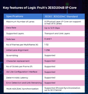
Logic Fruit has developed an RTL IP for JESD204B, and here we are showcasing several key features:
Benefits of JESD204B Interface
Following are some of the generic benefits of the JESD204B interface
- Reduced/simplified PCB area
- Reduced package size
- Comparable power for large throughput
- Scalable to higher frequencies
- Simplified interface timing
- Standard Interface
FAQS about JESD204B
1) How does JESD204B work?
The JESD204B standard offers an alternative to the more common parallel data transfers for integrating one or more data converters with a digital signal processing device (usually an ADC or DAC to an FPGA) via a faster serial interface.
2) What is the line rate of JESD204B?
12.5 Gbps
The JESD204B IP core can handle between 1-32 lane configurations and line rates of up to 16.1 Gbps when not characterized according to the JESD204B specification. It can also handle line rates of up to 12.5 Gbps when characterized according to the JESD204B specification.
3) What is the JESD204B interface?
The JESD204B interface standard considerably reduces the number of digital IOs required, which eases board layout, while supporting the high bandwidth required to stay up with today’s top high-performance, high-speed, and multi-channel applications.
4) What is the JESD204B FPGA IP?
Lane rates of up to 12.5 Gbps (characterized and certified to the JESD204B standard) and up to 19 Gbps (for Intel Agilex® 7 E-tile) and up to 20 Gbps (for Intel Agilex® 7 F-tile) (uncharacterized and not certified to the JESD204B standard) are among the main features provided by the JESD204B Intel® FPGA IP core.
5) How do you calculate the lane rate in JESD204B?
With both the source and load impedance defined at 100 Ω ±20%, the lane data rate is stated as falling between 312.5 Megabits per second (Mbps) and 3.125 Gigabits per second (Gbps). It is characterized as having a common-mode voltage level range of 0.72 V to 1.23 V with a nominal peak-to-peak differential voltage level of 800 mV.
6) What is the JESD204B standard?
JESD204B Standard at a Glance. A standardized serial interface between data converters (ADCs and. DACs) and logic devices (FPGAs or ASICs)
7) What is the speed of JESD204B?
In addition to the deterministic latency, the JESD204B version increases the supported lane data rates to 12.5 Gbps and divides devices into three different speed grades.
Conclusion
In summary, wireless communication systems, radar and sonar systems, high-speed data gathering, and other fields all make use of the flexible JESD204B FPGA technology. It is a vital piece of technology in today’s systems that need real-time data processing and analysis because of its capacity for high-speed data conversion, transport, and processing.
JESD204B defines the multigigabit interface as a necessary communications channel between data converters and logic devices to address the demands for faster data-processing capability in the applications of today and tomorrow. A crucial part of system design is figuring out which subclass your application requires.


![Advanced Driver Assistance System [ADAS] Everything You Needs to Know](https://www.logic-fruit.com/wp-content/uploads/2022/10/Advanced-driver-assistance-systems-Thumbnail.jpg)