

Introduction
To implement a specific design on an FPGA, several strategies can be followed while writing an HDL code. The number of resources used and their allocation will vary with the logic supporting the design. Every FPGA has a fixed number of programmable logic, I/O banks, and memory elements.
The CLBs (Configurable Logic Blocks), which are present as a part of programmable resources, contain flip-flops, Look-Up tables (LUTs), and multiplexers. These CLBs along with programmable routing can form a complex web of combinational and sequential circuits.
The LUTs mainly define the behavior of the combinational logic designed with a VHDL or Verilog code. It simply generates output based on the input combination. An LUT carries a customized truth table for every possible input. The results are already stored, which gets loaded as the FPGA is powered up.
The incoming sections are going to provide a brief understanding of manually estimating the number of LUTs required to implement a piece of HDL code on hardware.
What is a Lookup Table (LUT)?
A lookup table is, as its name implies, a real table that produces an output depending on the inputs. A lookup table that performs the same function as an AND gate may be shown in this example.
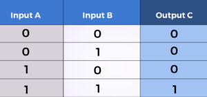
Try to picture this table being kept in a compact RAM right now. Address pins A, B, and C are inputs; data pin C is an input. Each time your address pins shift, they are pointing at a new address entry and “reading out” the result, which depends on the inputs and can be either 0 or 1.
Implementing MUX from LUT6
Let’s step forth with an easy example that depicts the schematic of a MUX obtained from Vivado tool. A single LUT6 contains 6 input pins and an output pin, which can be used to implement a 4:1 MUX (where 4 inputs + 2 select lines = 6 inputs).
Consider an example of MUX consisting of 4-bit input and 2-bit sel line and is implemented in HDL as
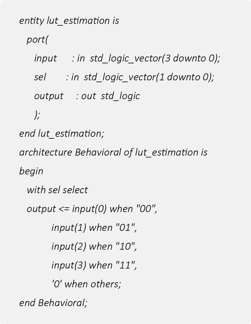
Then the Schematic would look as depicted by the below illustration.

Calculating LUTs
We have seen if the MUX input is 4 bits then it can be implemented using a single LUT6, but what happens if the input contains more than 4 bits? This will be implemented in different logic level levels.
Consider an input of N bits, now one LUT can accommodate 4 bits therefore N/4 LUTs can carry N bits, now N/4 output will be there in the first logic level (where all the outputs are evaluated simultaneously) and will travel to the next stage or logic level where we are gonna require (N/4)/4 (=N/16) LUTs to process N/4 inputs. This process continues until we get 1 as our final number. Then we simply add all the LUTs required in all the logic levels.
if N is not divisible by 4 then we will take the smallest integer value of (N/4).
Let’s consider an example of 128:1 MUX
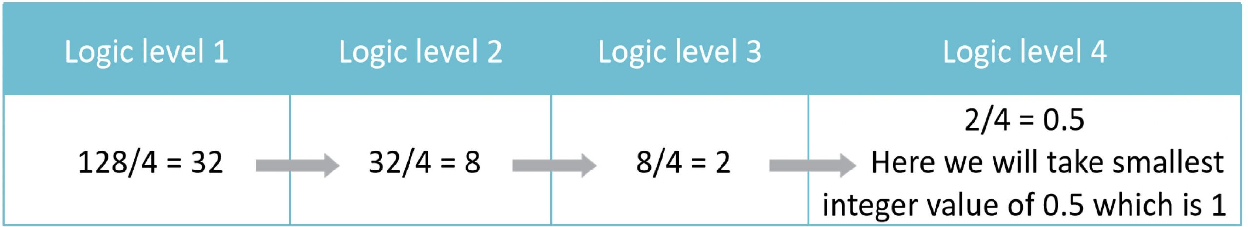
Total required LUTs = 32+8+2+1 = 43.
N will only include those bits of input on which the output depends. In this above example of 128:1 MUX, we have considered that two inputs among the six, are already occupied by select lines. If it isn’t the case then we will divide the integer N by 6.
LUT inputs may vary as different input LUTs are present on the FPGA. Some have 4 inputs whereas others have 6 inputs. Thus, the number dividing N will vary with the type of LUT.
Examples
Here, we will look into some examples and compare the LUTs count calculated from the above-mentioned formulae and the value estimated by Vivado tool.
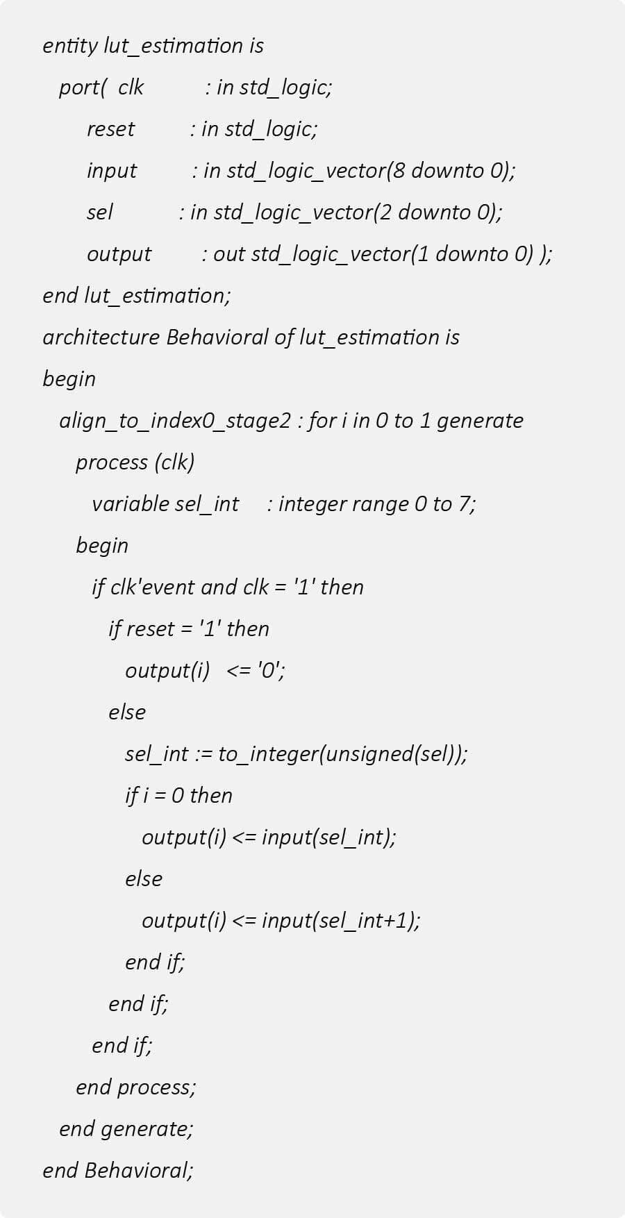
8-bit input and single-bit output
Consider an 8-bit input sequential circuit, where the output will be decided by the status or value of “sel” signal. Based on the current value of “sel” signal, the corresponding value of input will be taken out as output.
HDL Simulator evaluation:
The below mentioned diagram depicts the behavior of the above code, and here one can see that 3 LUTs and 1 flip-flop are needed, and 2 logic levels are present.

Mathematical Calculation:
Total LUTs required = (8/4) + LIF(8/16) = 2 + 1 = 3, where LIF is the least integer function or Ceiling function. Here we got 1 as our final quotient after two times division by 4, so logic level count will be 2.
8-bit input and two-bit output
Consider a 8 bit input sequential circuit, where output will be decided by the status or value of “sel” signal. Here, output is a 2 bit function.
Mathematical Calculation:
Total LUTs required = LUT[output(0)] + LUT[output(1)] = 2*[(8/4) + LIF(8/16)] = 2*[2 + 1] = 6, where LIF is the least integer function or Ceiling function. The logic level count is also 2 here.
HDL Simulator evaluation:
(when output(0) and output(1) depends on different values of input)
Here, despite the input being (8 downto 0), the output(0) and output(1) depend only on 8 bits of input but the inputs are different for both, therefore in the manual calculation we take N = 8.
The below mentioned diagram depicts the behavior of the above code, and here one can see that 6 LUTs and 2 flip-flops are needed, and 2 logic levels are present, and this matches with our mathematical calculation.

(when output(0) and output(1) depends on same values of input)
Here, the output(0) and output(1) depend on only eight-bit input and in a similar fashion.

Below mentioned diagram depicts the behavior of the above code, and here one can see that 4 LUTs and 2 flip-flops are needed, and 2 logic levels are present.

Here the LUTs are found to be lesser than the calculated value, this is, maybe, because of the capability of the tool to minimize the LUT by resource sharing as the output(0) and output(1) are sharing the same LUTs in the first logic level.
Uncertainty in calculating LUTs
Sometimes LUTs count could be different from the calculated value, and it is because of the resource sharing (as explained above) or due to the introduction of other resources, like MUX, etc., during resource management.
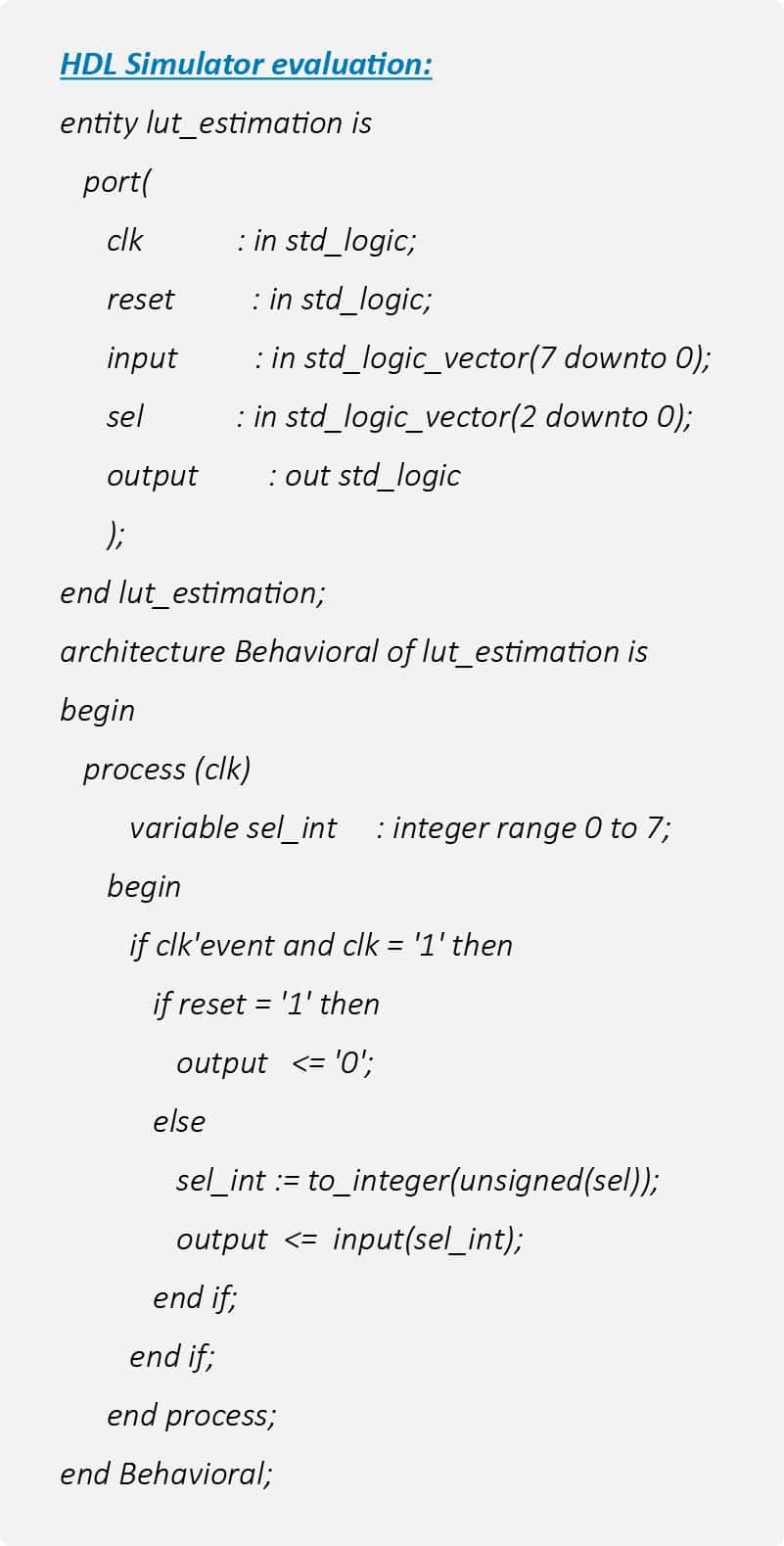
Consider a 128-bit input sequential circuit and a single output signal
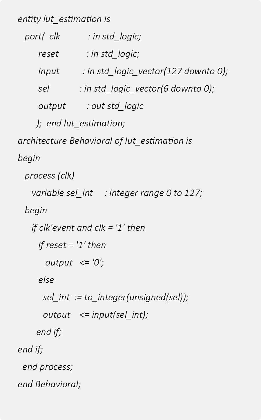
For the above-mentioned code:
Calculated LUTs = (128/4) + (128/16) + (128/64) + LIF(128/256) = 43
But the LUT count from vivado simulator was 35 because, at the second logic level, 2:1 MUX were used in place of LUTs.
Conclusion
Only provided with the set number of programmable and memory resources, sometimes it becomes crucial to keep the used LUTs count in check. Mathematical calculation could give us a rough estimate of possible LUT count for a given HDL code, and this value may vary among different tools or different versions of the same tool as they have their own defined way of allocating resources.
If your current HDL design has put forth an unprecedented situation, and you are looking for solutions, Logic Fruit Technologies can help you find them. Right from planning the entire schematic to optimizing the final design, Logic Fruit can assist you in every possible way. We have developed timing and resource-optimized data paths, supporting bandwidths up to 2Tbps, in FPGAs.
Logic Fruit Technologies is driven by more than a decade of experience in high-speed protocols and interfaces, including 1G/10G/40G/100G Ethernet, PCIe(Gen1-Gen6), USB3.0/4.0, CPRI/ORAN, Display Port, ARINC818 etc, and are well equipped to facilitate every design requirement.
FAQs
1) What are FPGA LUTs?
With the hardware resources available on FPGA, any digital system may be designed. Lookup tables, or LUTs, are one type of them. The fundamental FPGA building block, or LUT, offers us the possibility of reconfigurable computing.
2) What are LUTs in VHDL?
The behavior of the combinational logic created using a Verilog or VHDL code is mostly defined by the LUTs. All it does is provide an output depending on the combination of inputs. A unique truth table is carried by a LUT for each potential input. The results are pre-stored and loaded upon powering up the FPGA.
3) How many LUTs are in an FPGA?
Lookup Tables (LUTs)
The concept of operation is the same even though this example shows a 3-input LUT for simplicity, even though standard FPGAs normally utilize 6-input LUTs.
4) Why use LUTs instead of gates?
Reloadable, the LUT can implement any function of its inputs. Conventional logic gates are designed to do a single task. FPGA needs to have the freedom to freely reorganize its cells, and you want as much flexibility as possible. Furthermore, LUT is the best option.
5) How does an FPGA LUT work?
A unique truth table is stored in an FPGA’s LUT and is loaded at chip power-up. Consider the LUT to be a little RAM scratchpad. The address lines for a corresponding one-bit-wide RAM cell are the LUT inputs.
6) How is a lookup table implemented in an FPGA?
In an FPGA, a lookup table is usually implemented as a block of programmable logic. The programmable interconnect points of the FPGA are connected to the input variables, and the intrinsic logic of the LUT generates the output value.
7) How is a lookup table different from a programmable logic element (PLE)?
An FPGA can employ a programmable logic element (PLE) to implement a Boolean function. PLEs are a kind of digital circuit. A PLE is made up of a few configurable gates, like AND, OR, and NOT gates, that together perform a certain function. In contrast, a lookup table does not employ gates to accomplish the job; instead, it is made up of a list of input variables and their matching output values.
8) What are the advantages of using lookup tables in FPGA design?
The flexibility to implement any Boolean function, their simplicity and convenience of usage, and their ease of reconfiguration are some benefits of employing lookup tables in FPGA design. Since they don’t need gates to do the function, they are also typically faster than PLEs.