Introduction
ADCs and DACs, two components of high sample rate data converters, have higher requirements than serial interfaces can handle.
High throughput data transfer from fast-sampling ADCs would be possible over LVDS lines, which would offer high data rates over differential pairs to a single device.
The JESD204 specification was later published by JEDEC, and numerous components have since used it as a data converter interface.
Fast ADC/DAC components that sample signals at very high sample rates may now handle extreme data rates thanks to the latest version of the JESD204 interface standard, known as JESD204C.
With just over two years having passed since the release of the most recent version of the standard, a wide range of parts are now on the market that may be combined with FPGAs to enable ultra-fast DSP, transmission, and sampling in radio frequency systems.
This blog presents JESD204C, outlines its advantages and characteristics, and emphasizes how it differs from JESD204B, its predecessor.
Overview of JESD204C
JEDEC publishes and maintains the general JESD204 standard, which is updated with the JESD204C standard. The purpose of the standard is to eliminate the need for LVDS lines to be used between data converters and their system hosts.
It describes a serial interface and protocol used for signal synthesis, synchronization, and sampling in high-sample rate ADCs and DACs. This interface’s synchronization feature is crucial since it enables a single host controller to coordinate signal synthesis and sampling across numerous devices.
The encoding properties and data rate of the previous JESD204B iteration, which employed 8b/10b encoding with a maximum data rate of 12.5 Gbps, are improved in the JESD204C iteration.
ADCs and DACs that run at speeds between 100 Mbps and 1 Gbps or greater typically have this interface.
Evolution from Previous Versions (JESD204A and JESD204C)
JESD204 (2006)
The initial release of JESD204 was in April of 2006. A multi-gigabit serial data link between converter(s) and a receiver—typically a device like an FPGA or ASIC—is described in the standard.
A single serial lane connecting a converter or several converters to a receiver was the definition of the serial data link in this edition.
The physical interface, represented by the lane, is made up of a differential pair of interconnects that use current mode logic (CML) to connect the M number of converters to the receiver.
The serialized data link that is created between the converter(s) and the receiver is represented by the link. The frame clock serves as the clock for the JESD204 link between the converter(s) and the receiver in addition to being routed to both of them.
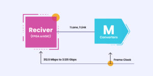
The source and load impedance are both stated as 100? ±20% and the lane data rate is defined as falling between 312.5 Megabits per second (Mbps) and 3.125 Gigabits per second (Gbps).
It is characterized as having a common-mode voltage level range of 0.72 V to 1.23 V with a nominal peak-to-peak differential voltage level of 800 mV.
To avoid routing an extra clock line and the accompanying complication of aligning an additional clock signal with the transmitted data at high data rates, the link uses 8b/10b encoding, which has an integrated clock.
Comparing this type of serial data transfer to synchronous-sampling parallel LVDS and CMOS interface designs, a trace-to-trace tolerance relaxation is possible.
Furthermore, the encoding is DC balanced, which ensures a substantial transition frequency for applications involving clock and data recovery (CDR) architectures.
Additionally, data and control characters that define link alignment, upkeep, and monitoring can be used thanks to the encoding.
To align the data on the lane between the converter(s) and the receiver over the connection, the standard provides training patterns using these control characters.
The receiver keeps track of the link’s quality and establishes and drops connections by the JESD204 standard’s specified error thresholds.
When supporters realized that the standard required to enable multiple, aligned serial lanes with numerous converters to handle converters with ever-increasing speeds and resolutions, they changed it accordingly.
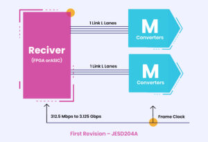
JESD204A (2008)
The initial version of the standard, known as JESD204A, was published in April 2008. The ability to handle multiple aligned serial lanes with multiple converters was added to the standard in this iteration.
It continued to handle the same lane data rates as the original standard, which ranged from 312.5 Mbps to 3.125 Gbps, as well as the same frame clock.
The standard’s ability to support multiple, aligned serial lanes was expanded, enabling converters with high sample rates and high resolutions to reach the 3.125 Gbps maximum supported data rate.
Higher sample rates and/or higher resolution converters could be supported by incorporating these features within the standard.
For instance, transmitting over one link with one lane as specified in JESD204 would require an output data rate of 5.0 Gbps for a 14-bit ADC running with a sample clock of 250 MHz.
The converter samples could now be mapped onto two aligned serial lanes, thanks to JESD204A’s modification, which also enabled multiple aligned serial lanes.
As a result, the data rate would drop to 2.5 Gbps per lane, which is less than the 3.125 Gbps maximum supported data rate.
To accurately duplicate the sampled signal in the analog domain once the signal has been received, it is crucial to understand the temporal relationship between the sampled signal and its digital equivalent while working with an ADC.
A crucial component was still missing from both the original JESD204 standard and the updated JESD204A standard, despite their superior performance over traditional interfaces: predictable latency in the serialized data on the link.
The ADC’s latency, which is the number of clock cycles from the moment the input signal’s sampling edge occurs until its digital representation appears at the ADC’s outputs, has an impact on this timing connection.
The deterministic setting of the ADC’s latency and its serialized digital outputs was absent from the JESD204 and JESD204A standards.
Additionally, the speed and resolution of converters were getting faster. Due to these causes, JESD204B, the second revision of the standard, was introduced.
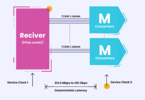
JESD204B (2011)
The second and most recent version of the standard, JESD204B, was published in July 2011. The addition of clauses to provide deterministic latency was one of the updated standard’s main elements.
Furthermore, 12.5 Gbps was added to the list of supported data rates, with descriptions of various device speed grades provided.
The principal clock source should switch from the frame to the device clock by this standard edition.
Second Revision – JESD204B
There were no guidelines established in the first two iterations of the JESD204 standard to guarantee predictable latency throughout the interface.
The JESD204B revision addresses this problem by offering a way to guarantee that the latency should be predictable and repeatable both across link re-synchronization events and from power-up cycle to power-up cycle.
This is achieved by using an input signal known as SYNC~ to start the initial lane-alignment procedure in the converter(s) simultaneously across all lanes at a predetermined moment.
Furthermore, to accommodate for skews across the serial data lanes, the receiver needs to buffer each data lane. The Rx Buffer Delay (RBD), a programmable number of cycles, should be used to release these buffers concurrently and at a predetermined point in time.
JESD204C (2017)
To meet the increasing performance requirements for both this generation of multigigabit data processing systems and those of the future, the most recent modification of the standard, JESD204C, was released in late 2017.
Four overarching objectives were set by the JESD204C subcommittee for this new standard revision: lane rates should be increased to accommodate the demands of even greater bandwidth applications; payload delivery efficiency should be enhanced; and link robustness should be addressed.
Additionally, they intended to address some of the faults in the JESD204B version of the standard and provide a specification that was clearer than that one.
Additionally, it was intended that JESD204B have a backward-compatible alternative. JEDEC has the whole JESD204C specification available.
This two-part primer introduces the JESD204C standard by outlining its key features and differentiating it from JESD204B.
It also aims to meet the previously mentioned objectives of improving interface usability and providing the bandwidth capability required by a range of industries.
An overview of these modifications and the additional features is given in Part 1 of this series. We’ll go a little bit more into the most significant new features in Part Two.
Key Features of JESD204C
Delivering Performance
- Designed to JEDEC JESD204C.1 specification
- Line rates from 1 Gbps to 32.5 Gbps
- Supports 1-24 lanes
- Supports 1-96 converters
- HD-mode supported
- Performs user-enabled scrambling
- Generates initial lane alignment sequence
- Performs the alignment character generation
- Checks link configuration data with user-selected parameter values during the initial lane synchronization sequence
- 8b 10b, 64b 66b, 64b 80b encoding/decoding supported
- Verilog-based
- Optional data mapping and de-mapping
- Supports Subclasses (0, 1, and 2) on the 64b 66b link layer
Interoperability
- JESD204C IP has been interoperability tested with Analog Devices JESD204C implementation
Easy to use
- HW demonstration platform available
- VIP and regression test suite available
- A simple test bench is included
Silicon Agnostic
- Designed in Verilog and targeting both ASICs and FPGAs
New Terminology for JESD204C
In JESD204C, several new words and configuration settings are introduced, mainly to explain the functions related to the 64b/66b and 64b/80b link layers.
The terms and factors that are most pertinent are listed below, along with a brief explanation of each. These will be covered in more detail in the sections that follow.
Transport Layer
The transport layer from JESD204B is preserved for JESD204C. Eight-octet blocks of the data frames assembled in the transport layer are transmitted over the network.
This standard’s part has been reorganized, its wording has been clarified, and its figures have been updated.
There are various setups where the frame boundaries will not line up with the block boundaries (frames may not contain exactly eight octets) due to the nature of the 64-bit encoding techniques. The second installment of this series will go over the specifics and ramifications of this.
Data Link Layer
The various data connection layer approaches are covered in two main sections of the standard, as was previously mentioned.
As a backward-compatible option, the 8b/10b encoding method from earlier JESD204 standard versions is still in place. This includes the usage of the SYNC~ pin and K.28 characters for synchronization, lane alignment, and error monitoring.
Long-term, nevertheless, the majority of applications will probably make use of one of the new 64-bit encoding techniques included in JESD204C.
Based on IEEE 802.3, the 64b/66b method will offer the best efficiency. Even though it’s called encoding, there isn’t any encoding happening (as in 8b/10b).
The approach simply increases the 64 bits of payload data by two header bits. Given this, scrambling is required to preserve DC balance and to guarantee sufficient transition density, which is necessary for the clock and data recovery (CDR) circuitry in the JESD204C receiver to reliably recover the clock.
The second installment of this series will go into further detail on this. Additionally, a 64b/80b option has been created, allowing the use of new features like forward error correction while maintaining the same clock ratios as the 8b/10b scheme.
The 8b/10b encoding used in JESD204B is incompatible with both 64-bit encoding techniques.
Physical Layer
While keeping the lower limit of 312.5 Mbps set in previous revisions, JESD204C has raised the highest limit on lane rates to 32 Gbps.
JESD204B has a maximum throughput of 12.5 Gbps. 8b/10b encoding is not advised for lane rates beyond 16 Gbps, while it is not technically prohibited; neither of the 64b schemes is advised for lane rates below 6 Gbps.
Two class categories are introduced in JESD204C to specify the properties of the physical interface.
The Below table lists the lane rate associated with each class.
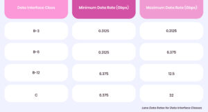
Lane Data Rates for Data Interface Classes
The Below table lists the channel types within Class C and the associated emphasis and equalization characteristics.

JESD204C 32 Gbps Interface Device Class Features
The JESD204 channel operating margin (JCOM), which is used to verify conformance with the Class C PHY layer standard, is another idea introduced by JESD204C.
The eye masks that use the Class B PHY layer implementations that are detailed in this and earlier versions of the standard are supplemented by this operating margin computation.
Clocking and Synchronization
The device clock and SYSREF specifications from JESD204B will still be used in JESD204C.
However, to offer a mechanism for deterministic latency and multichip synchronization, when employing either of the 64-bit encoding schemes, the local extended multiblock counter (LEMC) is aligned using the SYSREF rather than the LMFC.
The synchronization procedure employed in JESD204B is entirely distinct from that of the 64-bit encoding techniques.
Sync startup and error reporting will now be handled by application layer software, as the SYNC signal has been removed.
Consequently, neither the initial lane alignment sequence (ILAS) nor code-group sync (CGS) exists.
New words linked to sync that are used to describe the synchronization process are extended multiblock alignment, extended multiblock sync, and sync header sync.
These synchronization stages are all accomplished with the use of 32-bit sync words.
Deterministic Latency and Multichip Synchronization
As previously mentioned, the deterministic latency and multichip synchronization technique from JESD204B is mostly preserved.
There’s no option for Subclass 2 when utilizing one of the 64-bit encoding techniques. Rather, the SYSREF signal is utilized to align the LEMC across all devices in the JESD204 subsystem, and only Subclass 1 operation is supported.
Forward Error Correction
To achieve the objective of offering a more reliable link at faster lane speeds, JESD204C now provides an FEC option.
This approach, which may be especially helpful for instrumentation applications, is based on fire codes. You can only use this optional feature if you are using one of the 64-bit encoding schemes.
Cyclic codes, or fire codes, are used to fix single-burst faults. The benefit of cyclic codes is that their codewords can be expressed over a finite field as polynomials rather than vectors.
For quicker decoding, fire codes employ a symptom that may be divided into two halves.
Implementing the JESD204C Interface on an FPGA
The JESD204C standards control the data flow over the interface between an FPGA and an ADC, DAC, or MxFE.
The JESD204C protocol allows for lane rates of up to 32.75 Gbps, while the JESD204B protocol only allows for lane rates of up to 16 Gbps.
The 64-bit/66-bit encoding system used by JESD204C offers a significantly improved encoding efficiency and relies solely on feed-forward synchronization, doing away with the requirement for a handshaking procedure to establish initial connection synchronization.
The data path is depicted in the below diagram, which can be loosely divided into four layers, each of which carries out particular functions inside a design.
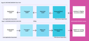
JESD204B/JESD204C data path layers
Some of the Critical points to look out for in the JESD204C Interface
Every protocol layer IP block from ADI’s high-speed data converters offers capabilities that can be set to aid in debugging the JESD204C interface after it is integrated into a system, in addition, to debug register fields and test modes.
PHY Layer Debug
Fast-rising and falling edges on high-speed signals traverse parallel lanes on a board at the physical interface between FPGAs and high-speed data converters.
There are two PHY layer debug spots that are advised for troubleshooting a JESD204C link.
Serializer Deserializer Clocking
The high-speed clock that powers the serial transmitter and receiver paths on the FPGA and high-speed data converters is generated by a phase-locked loop (PLL) synthesizer.
In the clock data recovery (CDR) circuit, the PLL is an essential block that is often driven by a reference clock that has a predetermined relationship to the line rate.
Both the FPGA IP and the ADI data converters can check for PLL lock. The PLL will unlock if this reference clock isn’t set at the correct rate.
Data Link Layer Debug
A synchronization sequence is required for the JESD204C link establishment procedure, and if it is not carried out correctly, the link establishment process will fail.
To make sure the link is formed for JESD204B use cases or designs, code group synchronization (CGS), initial lane synchronization (ILAS), and the physical sync signal must be watched over.
It is the extended multiblock (EMB) lock and the sample header (SH) lock in the instance of JESD204C. For the data link layer, two debug points are advised.
JESD204C Mode Mismatch
The FPGA and the data converters must be configured in the same mode since the chosen mode (L, M, F, S, K, and other parameters) controls how the link layer encodes and decodes the data delivered over the interface.
Make sure the JESD204C parameters are configured correctly if there are discrepancies in the data that are not originating from the physical link.
JESD204C Lane Mapping Mismatch
It can be difficult to route the fast physical parallel lanes between the data converter and the FPGA. The limitations on routing can be loosened by using a crossbar that permits routing physical lanes to logical lanes on a receiver and logical to physical lanes on a transmitter.
A lane mapping mismatch could cause the link not being formed if a lane mapping crossbar is used; verifying mapping could be a useful diagnostic step.
Transport Layer Debug
The translation of lane data into sample data is the responsibility of the transport layer. There is a single suggested debugging method for situations when the data output from the transport layer is inconsistent.
Pattern Mode
The integrated test modes of ADI’s ADCs may produce a variety of predefined and user-defined digital patterns.
These patterns are ideal for identifying problems in the FPGA receive transport layer since they are simpler to understand on the output.
It can also be useful as a debug step when the FPGA transmit transport layer is in charge of producing the correct lane data from sample data by feeding it with a predefined pattern.
Error Monitoring
The FPGA IP modules and high-speed data converters can indicate any faults on the link as the data is being transported or received, in addition to establishing the link.
This information adds another layer of system debugging and is useful for link monitoring.
Applications
Almost any system that uses data converters operating at high gigabit and megabit data speeds can benefit from the JESD204C interface. A selection of the applications consists of
- Test instruments
- 5G cellular equipment
- Other cellular base-station gear
- Medical Apparatus
- Military/electronic warfare (EW)
- Satellite
- Almost any direct-conversion software-defined radio (SDR)
Benefits of JESD204C
- With the addition of error correction(FEC), cutting-edge instrumentation and other applications can operate without any errors.
- Offers better DC balance, clock recovery, and data alignment compared to JESD204B.
- The bit overhead is 3.125% which is much smaller than JESD204B (~ 25%).
- Provides an interface for serializing devices from some system designs, reducing space, power, and cost.
- It supports interface requirements of high megabit and Gigabit data rates for various applications such as 5G cellular equipment, test equipment, medical devices, military warfare, and so on.
- Mechanism to achieve Deterministic latency across the serial link
Logic Fruit’s JESD204C IP Core Features:
Logic Fruit has developed an IP Core designed specifically for JESD204C, and here are some of the IP Features of Logic Fruit’s JESD204C IP Core
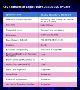
For further information about our Logic Fruit’s JESD204C IP Core, please visit our page by clicking here
JESD204B and JESD204C Compared
With its widespread adoption, the JESD204B standard was truly revolutionary. It delivered deterministic latency, 8B/10B encoding, multiple lane capability, and a data rate of 12.5 Gbps.
Along with a few new features like deterministic latency, 64B/66B encoding, and 32.5-Gb/s data throughput, the JESD204C standard has all the features of its predecessor.
The 64B/66B encoding is the main addition to the standard. Additionally, a 64B/80B encoding option is supported.
The 8B/10B encoding scheme, which was employed in the previous B version of the standard, entails first converting each of the eight bits that need to be conveyed into a distinct 10-bit value.
There are two valid justifications for this kind of encoding:
- More bits and bit transitions that aid in clock recovery and data stream alignment are now present in the encoded character.
- The average dc on the line is guaranteed to remain constant by the encoding. A variable or wandering DC average on the transmission path due to random bit counts might result in bit errors and other operational features.
Although 8B/10B encoding has advantages, it also causes transmission latency. It takes longer since ten bits are sent as opposed to eight.
The net data rate (R = 1/t) is 20% smaller than the data rate (R), even though R is still dependent on the bit time (t).
JESD204C uses the 64B/66B encoding standard. Along with bettering DC balancing, clock recovery, and data alignment, it also has a bit overhead of 3.125%, which is significantly less than that of the 8B/10B approach.
Before encoding, there is a scrambler in the signal processing. A digital circuit known as a scrambler converts the serial data into a highly randomized form.
It employs an algorithmic procedure based on a polynomial, in this case 1 + x14 + x15, much like a cyclic redundancy check (CRC). After scrambling, a serial digital signal with a spectrum that significantly lowers EMI generation is produced.
FAQs about JESD204C
1) What is the protocol for JESD204C?
A high-speed ADC/DAC interface protocol called JESD204C is used to communicate between data converters and other devices like FPGAs and ASICs.
The goals of JESD204C’s design were to decrease the amount of data lanes in these interfaces, streamline PCB layout, and increase power efficiency.
2) Is JESD204C backward compatible?
JESD204C has some restrictions on subclass-0 operation, however, it is backward compatible with both the A and B standards.
Designers who are acquainted with the JESD204B revision will notice compatibility based on the coding scheme and suggestions for increased throughput through the use of different standard upgrades.
3) What is the difference between JESD204C and JESD204B?
JESD204C has some restrictions on subclass-0 operation, however, it is backward compatible with both the A and B standards.
Designers who are acquainted with the JESD204B revision will notice compatibility based on the coding scheme and suggestions for increased throughput through the use of different standard upgrades.
4) What is the speed of JESD204C?
While keeping the lower limit of 312.5 Mbps set in previous revisions, JESD204C has raised the highest limit on lane rates to 32 Gbps. JESD204B has a maximum throughput of 12.5 Gbps.
5) What is the lane rate for JESD204C?
Choose the subclass modes for JESD204C. For each lane, determine the lane rate. 28.9 Gbps is the maximum rate. For additional information, see Performance and Resource Utilization.
Conclusion
In the next few years, JESD204C will define the multigigabit interface as a necessary communications channel between data converters and logic devices to meet the quicker data processing demands for data-intensive applications.
Ultra-high bandwidth applications are made possible with no overhead because of the 64b/66b encoding and up to 32 GSPS lane rates, which increase system efficiency.
These and other standard changes will help applications such as electronic warfare, radar, and 5G communications.
Modern instrumentation and other applications can rely on mistake-free operation for many years with the addition of error correction.


![Advanced Driver Assistance System [ADAS] Everything You Needs to Know](https://www.logic-fruit.com/wp-content/uploads/2022/10/Advanced-driver-assistance-systems-Thumbnail.jpg)