Introduction
Design entry, synthesis, implementation, and device programming are just a few of the stages or phases in the FPGA design flow.
The implementation stage involves selecting and configuring an IP address, as well as creating the RTL and limitations.
The implementation creates the file needed to program the device by using synthesis and place and route to develop the design.
It is possible to create iterative loops in the implementation process.
This blog covers the various implementation phases, identifies difficulties that require extra attention, and provides guidance on how to identify and eliminate bottlenecks.

FPGA Design Synthesis
Logic synthesis is one of the most critical processes in the Computer-Aided Design (CAD) flow for a Field Programmable Gate Array (FPGA) based design.
It usually comprises a series of optimization rounds aimed at enhancing the Quality of Results (QoR).
Aside from the traditional optimization objectives (e.g., performance, area, and power),
reliability has become a serious issue as modern FPGAs have advanced to 16nm and below technology, owing to reductions in core voltage, decreases in transistor shape, and increases in switching speed.
Synthesis takes RTL and time limitations into account to provide an efficient netlist that is functionally equal to the RTL.
In general, the synthesis tool may generate logic for any valid RTL. Synthesis necessitates realistic time constraints.
The Vivado ® Design Suite or any other similar EDA tools available can be used to carry out the synthesis procedures outlined in the following sections, each with its own set of benefits and trade-offs.
- Global Synthesis: In the global synthesis technique, the entire design is synthesized in a single run. Allows the synthesis tool to optimize to the best level possible. Because the synthesis tool has a thorough understanding of the design, it can optimize across hierarchies in a way that other procedures might not. When the synthesis is finished, it allows for easy analysis. This flow has the disadvantage of taking longer to compile. Every time synthesis is performed, the entire design is repeated. However, gradual synthesis can be used to alleviate this problem.
- Block Design Synthesis: The block design synthesis procedure can be used to create complicated systems using custom and Xilinx IP. In this stage, the Vivado IP integrator is used to create a Block Design File (.bdf). The system is connected when the custom IP address is added to the .bdf file. It manages to fit a lot of functionality into a small package. Allows for a greater focus on the entire system rather than individual components. Allows for increased design setup and synthesis speed.
- Out-of-Context Synthesis: In the Out-of-Context (OOC) synthesis flow, certain tiers of the hierarchy are synthesized separately from the top level. The Out-of-Context hierarchy must first be synthesized. Following that, top-level synthesis is carried out, with each out-of-context run treated as a black box. The EDA Design tool puts the design together from all of the synthesis runs when you access the top-level synthesized design after all of the Out-of-Context and top-level synthesis runs are completed. The time it takes to build the code for future synthesis operations is slashed in half. Only the runs you choose are resynthesized; all other runs are left alone. Stability is assured when design changes are made. In the runs, just the changes are resynthesized. The disadvantage of this approach is that it necessitates additional preparation. Be cautious while selecting which modules to employ as out-of-context synthesis modules. Any further XDC constraints must be established separately and used just for out-of-context synthesis.
- Incremental Synthesis: The incremental synthesis method could be utilized to take advantage of prior synthesis findings. Compile times for traditional synthesis have been sliced in half. When used in conjunction with the incremental implementation strategy, it improves overall compilation performance and temporal closure consistency. Incremental synthesis is most useful when the top-level design is RTL and RTL makes up a major portion of the design. In this mode, the amount of time it takes to build synthesis is lowered, and the outputs are reused. For designs involving a large number of block designs, IP, or both, the Vivado tools automatically break synthesis into these blocks and execute it in out-of-context (OOC) mode. As a result, incremental synthesis is less effective in these situations. Incremental synthesis reduces compile time by using unmodified hierarchies from the reference synthesis cycle. For incremental synthesis to work, the design must have at least 5 partitions with at least 10000 instances. Furthermore, any design changes should influence as few divisions as possible and should not take place at the highest level of the design.
Implementation
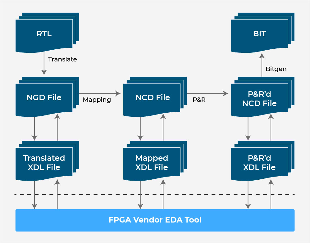
The implementation includes all methods required to deploy and route the netlist onto device resources while meeting the design’s logical, physical, and temporal restrictions. This procedure employs a three-step approach.
- Translate process: During the translation process, all of the input netlists and limitations are integrated into a logic design file. This information is saved in a Native Generic Database (NGD) file. This can be done with the NGD Build program. Setting constraints can include assigning ports in the design to physical parts (such as pins, switches, and buttons) of the desired device and outlining the design’s time needs. This information is saved in a User Constraints File (UCF file). The UCF is generated or altered using Pinout Area Constraints Editor (PACE), Constraint Editor, and other tools.
- MAP process: The MAP approach divides a circuit comprising logical elements into subblocks that can be stored in an FPGA’s logic blocks. That is, the mapping procedure converts the logic in the NGD file to FPGA parts (Combinational Logic Blocks (CLB), Input-Output Blocks (IOB)) and generates a Native Circuit Description (NCD) file that physically replicates the design. This is performed by employing the MAP program. In addition, a Physical Constraints File (PCF) including all constraint-related data is created.
- Place and Route: The Place and Route (PAR) software are used to carry out this technique. Based on the constraints, the place and route process connects the logic blocks and inserts sub-blocks from the mapping process into logic blocks. If a sub-block is placed near an IO pin in a logic block, for example, it may reduce time but impose additional limitations. As a result, the Place and Route technique take into account a tradeoff among all of the constraints. The PAR tool accepts a mapped NCD file and outputs a fully routed NCD file. The output NCD file contains the routing information.
The hardware utilization summary may not match after synthesis and the MAP procedure.
The MAP process employs several optimization techniques to minimize or reduce redundant, duplicated and underused logic components.
The maximum frequency obtained after the synthesis and MAP operations can be matched by smaller designs.
For sophisticated designs, however, the frequency acquired after the MAP process is often lower than that produced after the synthesis process.
The maximum frequency is determined by the total delay time, which is calculated as:

Total Delay = Data Path Delay (Logic Delay) + Clock Path Skew + Clock Uncertainty + Routing Path Delay
Design closure
Design closure occurs when all timing, system performance, and power criteria are met, as well as hardware functioning is adequately verified.
Design closure takes numerous iterations between results analysis, design change, and constraint modification.
When it comes to design closure, timing and power optimization are typically seen as trade-offs.
On the other side, many time improvements benefit power. For example, reducing the distance between cells reduces both propagation latency and connection power.
Timing Closure
To be deemed timing closed, the design must meet all timing criteria.
Reaching time closure is significantly easier if you have the right HDL and limitations for synthesis.
Furthermore, improved HDL, constraints, and synthesis choices must be cycled through the steps of synthesis.
To appropriately close timing, follow these general criteria:
- Look at how you’re doing throughout the flow if you’re having problems keeping time initially.
- The key to improving Total Negative Slack (TNS) is to focus on each clock’s Worst Negative Slack (WNS).
- Look for significant Worst Hold Slack (WHS) breaches to detect missing or inappropriate limits (-1 ns).
- Reconsider the trade-offs between design choices, constraints, and target architecture.
- Recognize the tool options as well as the design parameters.
- Make sure the tools don’t try to improve timing (extra margin) after the time limit has been met.
Power Optimization
The power consumption must be monitored and verified regularly as the design flow progresses through synthesis and implementation.
It ensure that thermal dissipation stays within budget, the board voltage regulators stay within their current operating limits, and the design stays within any system power limits.
If your electricity bill is approaching your budget, you can take quick measures to reduce it.
If the projected power consumption exceeds your budget, you must reduce power consumption by taking the steps suggested in the sections below.
- Analyzing Power Estimation: Examine the overall power in the Summary section. Is there room for total power and junction temperature in the thermal and electrical budgets? If the results are significantly above budget, look at the power summary distribution by block type and power rails. This will show you which blocks consume the most electricity. Review the Hierarchy section. The hierarchy breakdown gives a good idea of which module consumes the most power. Drilling down into a certain module can reveal the functioning of a block. You may also use the GUI to cross-probe individual modules to examine how they’re built and whether there are any power-saving approaches to recode them.
- Run Power Optimization: Power optimization can be done either pre-place or post-place in the design flow, but not both. The pre-place power optimization phase’s purpose is to conserve as much energy as feasible. This can cause problems with timing (in rare circumstances). If speed is the most important factor, Xilinx recommends the post-place power optimization phase. At this level, just the power optimizations that keep the clock ticking are done.
- Impact of Power Optimization: The purpose of power optimization is to limit the impact on timing while maximizing the amount of energy saved. However, if timing decreases as a result of power optimization, you can compensate in a few ways. When possible, use the set power opt XDC command to detect and apply power optimizations only to clock domains or modules that are not timing sensitive. Look at critical pathways to see if any cells have the IS CLOCK GATED property set to TRUE, indicating that the paths were optimized for power, whether the most critical clock domain spans a large portion of the design or uses the most power. In a future version, use the set power opt XDC constraint to disable power optimization on the power-optimized cells in the critical path to improve timeliness at the cost of more power. The implementation can then be restarted using the set power opt XDC limitations or Tcl commands.
Configuration and Debug
When the design has been successfully implemented, the following step is to load it into the device and execute it on hardware.
Configuration is the process of loading application-specific data into the device’s internal memory.
Debugging is required if the design fails to meet hardware requirements. It’s now time to program the FPGA using the design.
The design, on the other hand, must be converted into an FPGA readable format.
The BitGen software handles the conversion.
The routed NCD file is then used to generate a bitstream (a.bit file) that can be used to set up the target FPGA device with the BitGen software.
This can be accomplished with the use of a cable.
To load bitstream into the device, one of the following methods can be used:
- Direct Programming: The bitstream is loaded directly onto the device through a cable, processor, or custom solution.
- Indirect Programming: The bitstream is stored on external flash memory. Following that, the bitstream is loaded into the device through flash memory.
In-system debugging allows you to test your design in real-time on your target device.
You’ll need to do this if you run into scenarios that are tough to duplicate in a simulator.
For debugging, you provide dedicated debugging IP to your design, which lets you view and handles the design.
After debugging, you can delete the instrumentation or custom IP to optimize performance and logic reduction.
Debugging a design iteratively is a multistage process.
It’s advised to break down the design debugging process into smaller segments, concentrating on getting smaller components of the design to work one at a time rather than attempting to get the entire design to work at once, as is the case with the most difficult challenges.
The following are the steps to debug:
- Probing: Determine which signals in the design you’d like to look into and how you’d like to examine them.
- Execution: Execute out the design, which includes the debug IP for the investigated networks.
- Analyzing: Interact with the debug IP included in the design to troubleshoot and verify functional faults.
- Fixing phase: Make appropriate corrections and repeat as required.
FPGA Design: Best Practices for Team-Based Design is a book that explains how to build a successful FPGA Design.
Key areas of concern in implementing system designs have been identified, and a recommended design methodology to solve these issues has been developed, based on acquiring an understanding of their design environments, processes, and what works and what does not work.
One of the main R&D houses in the FPGA market, Logic Fruit Technologies, offers unique solutions to meet these workload demands and can serve any level of organization to give end-to-end solutions.
We specialize in high-performance real-time FPGA-software heterogeneous systems. Contact us to know more and let’s innovate together.