PCIe: As we have always known, the CPU has been the fundamental component of every motherboard ever since our introduction to computers. For the motherboard to function correctly, it is crucial that all the parts are in sync or, let’s say is, in a state of harmony This is where the PCI comes in.
The PCI ensures that all the motherboard components are working proficiently.
PCI stands for Peripheral Component Interconnect, used as expansion slots in a computer’s motherboard and acts as a pathway for communication between the motherboard and other devices.
The task of the PCI Express is to provide sufficient bandwidth to all these components to ensure an efficient connection with the system.
The PCI is a 32-bit bus which implies that it has 32 lines to transmit several data simultaneously at a good pace.
The introduction of the PCI brought a radical change in the overall working of expansion cards, majorly because of its Plug and Play feature. In the interim,
PCI allows for automatic resource configuration i.e. instead of manually configuring the expansion cards, they automatically request the resources it needs.
Learn More About: PCIe GEN6 Controller IP
How did PCIe come into existence?
Though the PCI was very well known, the speed limiting needed to be examined. To address the speed limiting problems, the PCI Express slot was introduced. PCIe stands for Peripheral Component Interconnect Express (PCI Express), a motherboard expansion launched back in 2003.
The PCIe enables high-speed serial communication between the CPU and all the other components of a motherboard.
Today, the PCIe has outperformed the PCI to become the primary expansion bus and a popular communication pathway for many other onboard applications and devices.
The primary reason behind introducing PCI Express was to enable a higher data transfer rate and simplify the overall system design.
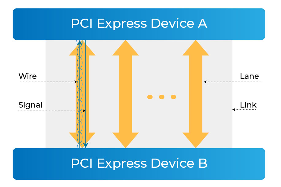
The PCIe standard has iteratively worked on over the long run from that point forward. Each new generation was designed explicitly to accommodate the latest bandwidth requirements of the cutting-edge computing system. The key feature of the PCI Express is the added lanes from 1 to 16 to increase its throughput.
PCI Express uses serial communication, unlike the PCI, which uses a shared bus for communication between the CPU and other peripherals.
What is PCIe?
PCIe stands for Peripheral Component Interconnect Express. It’s the term for this particular type of connection between a computer’s motherboard – or host – and peripherals – or endpoints – like graphics cards, sound cards, and expansion cards.
To connect them, one needs to just plug the PCI Express card into the PCI Express slot on the board.
The PCI Express was known as “High-Speed Interconnect” (HSI) at the early stage of its development. From various changes in its name like 3GIO (3rd Generation Input/Output) and PCI-SIG but at long last made due with the name PCI Express. PCI Express introduction came with several improvements that give it an edge over the older expansion bus standards. The internal components on a PC can be connected utilizing several different connectivity options, but the PCIe stands out of them all.
The PCIe standard provides access to improved and enhanced performance options with low latency.
The PCI Express architecture has filled in as the spine for I/O connectivity spanning three decades, enabling power-efficient, high-bandwidth, and low-latency communication between components.
PCI Express technology keeps on outperforming contending I/O advancements in terms of market share, capacity, and bandwidth and has continued as the omnipresent I/O interconnect across the entire compute continuum through its existence.
Its usage traverses various market segments such as hand-held, client, servers, workstations, data centers, High-performance computing, automotive, embedded systems, industrial applications, etc. PCI Express technology is so inescapable with its compelling power-efficient performance and cost-viability that other protocols, including ultra-latency sensitive load-store I/O protocols with memory, storage, and coherency semantics, run on PCIe PHY and leverage the PCIe infrastructure such as upper layers, software stack, and platform connectivity.
These improvements are credited to its prominence, and they include:
- The performance in regards to the scaling of the bus devices is higher.
- Its ability to detect and report errors is more prominent than other expansion bus standards.
- The pin count of the input /output is lower than its counterparts.
- It has a native hot-plug functionality implying that one can add a component without interrupting the system. The requirement for restarting isn’t required.
- It uses a serial communication method whereby only one bit is transferred on the data path per clock cycle.
Types of slots and cards
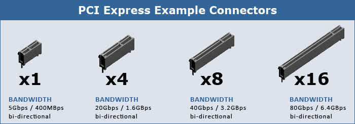
There are five standard PCIe slots and cards: x1, x2, x4, x8, and x16. The numbers represent the number of lanes on the card or slot. Very much like the lanes on the road, these lanes are paths for data to travel on. X1 has just one lane, x4 has four lanes, etc.
So, the more lanes, the more data can travel on them, and therefore the higher the potential rate of data transfer.
The number after X indicates the assortment offered by the PCIe interface concerned. Preferably talking, it would address the number of pins alongside the length of the connection.

A PCIe slot would depend on how many PCIe lanes it can provide access to. You should be able to use any pin-compatible devices on any other version. Nonetheless, using a higher generation connection on a lower generation device would lower the performance of the serial bus. Even the installation on any slots would be permitted and does work.
However, the return will be bottlenecked to the standard of the lower version. For instance, you can use the X8 card on an X1 slot, but you will not get the data transfer performance of X8, but it will be limited to X1.
PCIe Generations
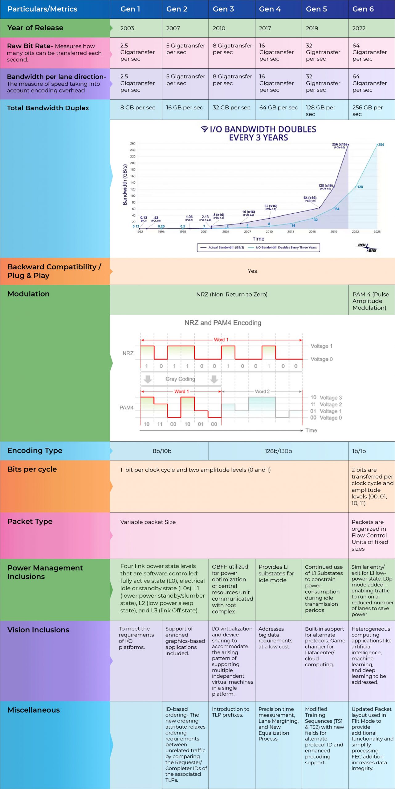
Six generations of the PCIe standard have been set up so far. The strong contrast between them is that the data transfer rate in each lane has doubled with each new generation. As we embark on the third decade with the 6th gen,
PCIe technology looks solid as the pervasive I/O interconnect over the whole compute continuum with its power-proficient performance and capacity to interface with hundreds of lanes, thereby connecting multiple devices in a platform. Currently, the available product is based on PCIe generation 4.0, and it offers up to 16 Giga transfers per second per lane.
Products with generation 5.0 are going to hit the market in this quarter itself as been updated by Samsung, which is going to launch its PCIe 5.0 SSD.
Talking about the latest generation of PCIe – the gen 6, its final specification has been published in the early week of 2022, so we could expect the product with gen 6.0 standards to strike through the market in 2023 or 2024.
#1. Gen 1:
PCIe technology got going in 2003 at a 2.5-GT/s in an encoded serial bit rate, supporting widths of x1, x2, x4, x8, and x16 for different bandwidth levels. The upheld widths haven’t changed through the six generations of evolution of PCIe architecture. While it uses an 8b/10b encoding scheme,
thereby incurring 25% encoding overhead, the PCIe 1.0 supports total bandwidth of 4 Gb/s. The 8b/10b encoding was needed to set up dc balance and for the additional required encodings for physical-layer packetization (e.g., to indicate start and end of different types of packets) and training handshake.
#2. Gen 2:
PCI Express 2.0 was launched in 2007 as a headway to PCI Express 1.1, with all new functional enhancements and the vision to support graphics-based applications. It came with a doubled transfer rate in comparison to the PCI Express 1 version. It additionally comes with improved-per-lane throughput from 250 Mbps to 500 Mbps.
The PCI Express 2.0 motherboard is entirely backward compatible with the PCI Express v1.x The PCI-SIG additionally asserted several improvements in the feature rundown of PCI Express 2.0 from point-to-point data transfer protocol along with the software architecture. Aside from this, the PCIe 2.0 standard enables slot power limits to change to allow for the higher-powered slots that support the latest high-performance cards. The encoding scheme continued to be the same as was used for gen1 and was supported by chipsets.
The PCI Express 2.0 standard provides faster signaling than the previous PCI Express versions, thus doubling the bit rate. This proved helpful for high bandwidth applications.
Apart from this, the faster signaling feature in the PCIe 2.0 standard allows for a narrow configuration in terms of interconnecting links, thus saving on costs. For instance, the PCI Express 1.x uses 8 links at a maximum bit rate of 2.5GT/s to provide a total bandwidth of 4GBytes/s.
The same bandwidth is achieved by the PCI Express 2.0 using just 4 links at a maximum bit rate of 5GT/s. Thus, the platform implementation cost is reduced while keeping up with the same performance.
#3. Gen 3:
In 2007, PCI-SIG had announced that the version of PCI Express 3.0 would be offering a bit rate of 8 Giga-transfers per second (GT/s). Besides, it was also supposed to be backward compatible with the current implementations of the existing PCI Express.
Now, you must be wondering that if the PCIe is considered to twofold its speed with every generation, then why there had been an increment to 8 GT/s, not 10GT/s. Here is the reasoning for the same. Moving to 10 GT/s introduced several challenges to the design community, such as:
- Possibility of changes in requirements to existing PCB materials and connectors
- Compromised electromechanical backward compatibility
- Possible reduction in the supported channel length
The decision to use a signaling rate of 8.0 GT/s was made to adapt to these difficulties. Eventually, PCI Express 3.0 does accomplish the objective of doubling the bandwidth, but using 8.0 GT/s only provides about 60% of the improvement.
The remaining 40% improvement is the aftereffect of removing protocol overhead. Half of the gain (20%) was accompanied by removing the 8b/10b encoding used in PCI Express 1.1 and 2.0 and replacing it with a 128/130b encoding scheme. This significant improvement has been achieved by a technical process alluded to as “scrambling,” whittling the overhead down to a modest 1.5%.
The removal of the K-codes and optimization of the protocol provided the last 20% needed for PCI Express 3.0 to double the bandwidth of PCI Express 2.0.
PCIe gen 3 was not just limited to delivering more incredible speed; it also supported elements like I/O virtualization and device sharing to oblige the emerging trend of supporting multiple independent virtual machines in a single platform.
To support the performance needs of accelerators, it added features, for example, caching hints, atomics, and lower-latency access through improved transaction bypass semantics.
It is supported by the CPU and mostly Intel CPUs, which is in sharp contrast to PCI Express 2.0, which was supported on chipsets. FX processors, however, do not support PCIe 3.0.
#4. Gen 4:
PCI-SIG officially announced PCI Express 4.0 on June 8, 2017. Quite a long time, huh, after the PCIe gen3 came? The journey to double the data rate from 8.0 GT/s to 16.0 GT/s took more time to ensure that platform and silicon ingredients could advance in a cost-effective and power-efficient way for a consistent innovation change.
The channel loss budget was expanded to 28 dB, which was 22 dB for gen3.
The routing material kept on improving with newer and economically feasible materials such as Megatron-2 (4 and 6) with improved loss characteristics, alongside enhancement in packaging technology, making it viable within the cost and power constraints of platforms with hundreds of lanes.
However, a question naturally arises: How did the systems manage with the I/O bandwidth needs when the technology transition from PCIe 3.0 to PCIe 4.0 specification took longer than expected due to the inflection points that had to be addressed? The answer is subtle.
Platforms that appeared with PCIe 3.0 architecture had about 40 lanes of PCIe technology coming out of every CPU socket. Just before the transition to PCIe 4.0 specification, the lane count per CPU socket expanded significantly, coming to up to 128 lanes per CPU socket in some platforms.
Thus, while the per-slot (e.g., x16) bandwidth didn’t increase, the aggregate I/O bandwidth increased 3X in platforms, both in terms of the number of lanes as well as measured I/O bandwidth. Overall, the slowdown in speed evolution from PCIe 3.0 to PCIe 4.0 architecture was mitigated by a width increase because of the flexibility offered by PCIe specification.
The ecosystem evolved naturally, so the speed transition was accomplished in a cost-effective and power-efficient manner.

Fundamental PCIe elements such as the encoding technique and target bit error rate (BER) remained consistent with Gen4. Signaling and scrambling schemes moreover remained reliable.
PCIe 4.0 technology allowed more outstanding transactions to sustain the ever-increasing bandwidth capabilities through scaled flow-control credit mechanisms and extended tags.
It additionally upgraded the reliability, availability, and serviceability (RAS) features to enable migration to direct-connected PCIe storage devices. PCIe gen 4 came with a newer DLLP functionality and proved to be a big game-changer in the Big data market.
To assist with the advancement of hand-held segments such as smartphones and tablets, PCIe gen 4 came with an enhanced low-power state by inculcating deeper low-power states.
This enabled devices to maintain their states for a quicker resumption of traffic while consuming power in the single digits of microwatts.
This mechanism for lower power consumption during idle state along with the industry-leading power efficiency during active state (around 5 pJ/bit), plus a fast transition time between the two (1 to 100 µs), results in PCIe architecture being the interconnect of choice across low-power as well as high-performance segments. As always, the PCIe gen 4.0 continued to be backward compatible with older generations.
#5. Gen 5:
The PCI Express 5.0 is almost the latest expansion interface launched back in 2019. The 5.0 is a resulting augmentation of the PCIe 4.0 that offers double the bandwidth, data-transfer rates, and frequency compared to all the previous generations.
It is fully backward compatible, permitting you to pair it with motherboards having either 1.0, 2.0, 3.0, or 4.0 slots, respectively. With the PCIe 5.0, you are looking at a higher data transfer speed of about 32 Gbps and a 128 Gb/s bandwidth in a 16-lane configuration.
PCIe 5.0’s5.0’s specs may be over the top excess for some, particularly for consumers as of now observe PCIe 4.0’s4.0’s performance an overabundance. So for what reason do we require PCIe 5.0?
Unlike in the consumer space, PCIe 4.0’s4.0’s specs miss the mark for new compute-demanding and data-intensive apps like those in data centers, AI, ML, and crypto-mining.
Additionally, cloud-based applications are becoming more noteworthy as more and more industries are shifting to the cloud. The quick reception of Artificial Intelligence/Machine Learning (AI/ML) applications and the move to cloud-based workloads have fundamentally expanded organization traffic as of late.
As the compute and memory capacity increases exponentially, we need to sustain I/O bandwidth doubling at an accelerated cadence to keep up with the performance of emerging applications. PCIe 5.0, with its native support for carrying additional protocols over its low latency non-return to zero physical layers, can help CPUs keep up with the ever-increasing flow of data from edge devices.
To know more about how the PCIe 5.0 is catering to the insatiable demand of Data Centers, read our blog “Focal Points of PCIe 5.0 Interface for Data Center Performance“.
The networking space also needed PCIe 5.0’s speed bump. Network providers need to stay ahead of the consistently growing demand for faster speed. 5G devices are starting to dominate the market, and giant companies have already addressed the need for 400G Ethernet while some have already made the shift.
PCIe 4.0’s4.0’s features, albeit currently strong, will soon not be enough to cater to the growing demand for faster network speed and higher bandwidth, thus the need to upgrade to the much faster PCIe 5.0.
For example, 400 Gb (or dual 200 Gb) networking needs an x16 PCIe at 32.0 GT/s to sustain the bandwidth, which can very well be addressed with PCIe gen 5.

The advancement from PCIe 4.0 to PCIe 5.0 specification was fundamentally a speed upgrade. The 128b/130b encoding, which was the protocol support to scale bandwidth to higher data rates, was already built-in with PCIe 3.0 and PCIe 4.0 specifications.
But, going to Gen5 needed to add greater capabilities under the hood for handling signal loss and noise.
This is on the grounds that going faster may encounter more signal integrity (SI) issues, and that needs to be accounted for to keep errors at bay as much as possible, leading to the use of better quality motherboard traces and thicker PCBs with more layers to minimize signal loss and impedance.
The channel loss was extended to 36 dB along with enhancements to the connector to reduce the loss with the increased frequency range.
One of the upgrades made with PCIe 5.0 architecture is the built-in support for alternate protocols. PCIe technology has evolved to be the highest bandwidth, most power-efficient, and most widely deployed interface. Some usages require additional protocols, such as coherency and memory, to run on the same pins as PCIe architecture.
#6. Gen 6:
As PCIe embarked on its third decade, it just debuted its sixth generation at 64.0 GT/s, as part of its evolution, doubling the bandwidth every generation while keeping up with full backward compatibility.
PCIe 6.0 specification requires critical upgrades to the package, connectors, and materials, as done with prior speed increases. Due to channel loss, there are also significant challenges to doubling the data rate beyond 32.0 GT/s of the NRZ (non-return to zero) method.
Thus, PCIe 6.0 specification uses PAM4 (Pulse Amplitude Modulation, 4 levels) signaling to achieve a similar channel reach as the PCIe 5.0 specification.
PAM4 uses 4 voltage levels to encode 2 bits of data. Networking standards widely adopted PAM4 when they moved to a data rate of 56 Gb/s and beyond. While PAM4 helps with the channel reach, it comes at the detriment of a much higher bit error rate (BER) compared to previous generations.

Despite the fact that PCIe architecture has a Link Level retry (LLR) mechanism to replay transactions impacted by error(s), the loss of bandwidth due to retry makes it untenable with PAM4 error rates. What can we do here? Queue the superhero music because this is where FEC comes into play.
FEC To The Rescue.
Living up to its name, Forward Error Correction (FEC) is a means of correcting signal errors in a link by supplying a constant stream of error correction data, and it’s already commonly used in situations where data integrity is critical, and there’s no time for retransmission.
While FEC hasn’t been necessary for PCIe until now, PAM4’s delicacy will change that. The inclusion of FEC shouldn’t have a perceptible effect on end-users, but for the PCI-SIG, it’s another design requirement to battle with.
In particular, the group needs to make sure that their FEC implementation is low-latency while still being appropriately robust, as PCIe users won’t want a significant increase in PCIe’s latency.
Thus, PCIe 6.0 specification uses a lightweight FEC in conjunction with the LLR mechanism to meet low latency and low bandwidth overhead performance metrics.
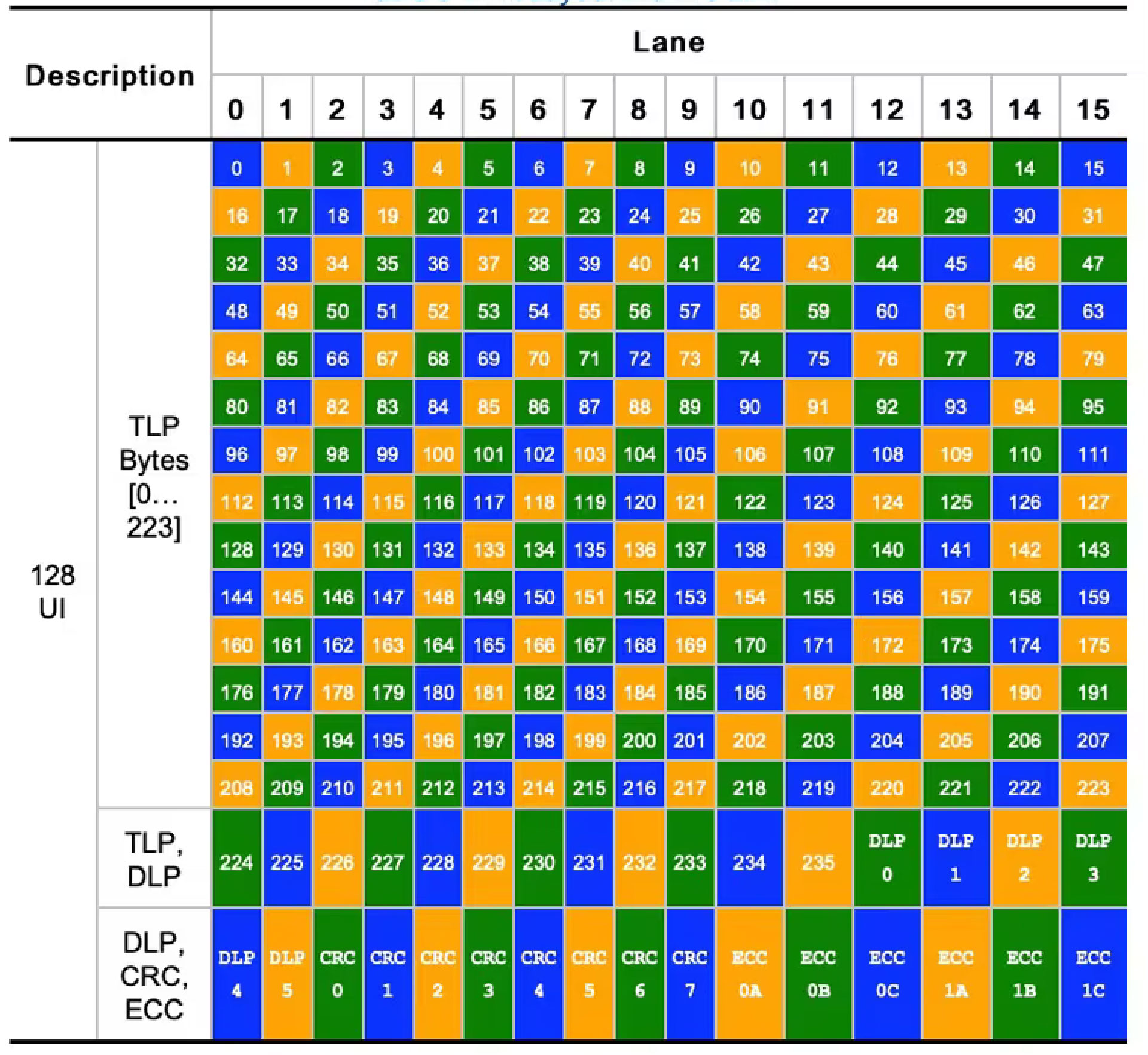
Alongside PAM4 and FEC, the final major technological expansion to PCIe 6.0 is its FLow control unIT (FLIT) encoding method. Not to be mistaken with PAM4, which is at the physical layer, FLIT encoding is employed at the logical level to break up data into fixed-size packets.
It’s by moving the logical layer to fixed-size packets that PCIe 6.0 is able to implement FEC and other error correction methods, as these methods require said fixed-size packets. F
LIT encoding itself is not a new technology, but like PAM4, it is essentially being borrowed from the domain of high-speed networking, where it’s already used.
PCIe Comparison:
Hence, PCIe is the protocol of choice for performance-hungry peripheral communications and is the go-to high-performance interconnect for the foreseeable future. At the same time, backward compatibility is a critical strength of the PCIe lineage.
This implies that irrespective of the particular version of the PCI Express your computer system or motherboard can uphold, they ought to be cooperating, basically at some base level.
PCI Express is a form of technology that is constantly under some sort of technical modifications. Since there is no expiry date for PCIe specifications, several generations can coexist in the marketplace and, surprisingly, in the same application.
This is an advantage for system designers: while successive new PCIe generations emerge to address increasingly bandwidth-hungry requirements, earlier iterations continue to deliver value in a large number of scenarios such as personal computing, gaming, and some enterprise computing and networking applications.
We have, as of now, got the substance that the PCIe upgrade isn’t simply restricted to speeding up or performance; it brings considerably more to the table. In addition to Bandwidth enhancement, the update to different versions of the PCI Express also tends to bring about effective bug fixes, additional technical features, and improved power management.
So, with this crisp and concise detailing, we are at our last section of this blog, the FAQs section. Here are some of the FAQs related to PCIe, which will be a supplement to your learning so far.
PCIe FAQs:
What is PCIe Enumeration?
PCIe enumeration is the process of detecting the devices connected to the PCIe bus.
As part of PCIe enumeration, switches and endpoint devices are allocated memory from the PCIe slave address space of the HOST.
The enumeration process includes:-
– Initialization of BAR address of endpoint and switches
– allocation and initialization of MSI/MSI-X address for the devices.
– empowers bus-mastering capabilities of the device to initiate transactions on the bus.
– Initialization of different capabilities of the devices like power-management, max-payload size, etc
What are the layers of PCIe?
PCI Express can be divided into three discrete logical layers: the Transaction Layer, the Data Link Layer, and the Physical Layer. Each of these layers is divided into two sections: one that processes outbound (to be transmitted) data and one that processes inbound (received) data.
What is PCIe Equalization?
When the PCIe link is at GEN3 or higher speeds, then there can be less signal quality (bad eye).
Equalization is the process of compensating for the distortion introduced by the channel. After passing through a band-limited channel, the high-frequency components of the signal are heavily attenuated, which distorts the signal and spreads it into subsequent symbol periods.
This is visible as a closed eye in the eye diagram. The process of equalization produces a sufficiently open eye, as in Figure 1, and decreases Inter Symbol Interference (ISI). This facilitates the easier recovery of transmitted symbols, ultimately reducing the Bit Error Rate (BER). The Link equalization procedure enables components to adjust the Transmitter and the Receiver setup of each lane to improve the signal quality (good eye). The equalization procedure can be initiated either autonomously or by software.
What is trainable equalization?
Trainable equalization refers to the ability to change the tap coefficients. Each Tx, channel, and Rx combination will have a unique set of coefficients yielding an optimum signal-to-noise ratio. The training sequence comprises adjustments to the tap coefficients while applying a quality measurement to minimize the error.
What is scrambling?
PCI Express utilizes data scrambling to diminish the chance of electrical resonances on the link. PCI Express specification defines a scrambling/descrambling algorithm that is carried out utilizing a linear feedback shift register.
Scrambling is a technique where a realized binary polynomial is applied to a data stream in a feedback topology. Since the scrambling polynomial is known, the data can be recovered by running it through a feedback topology using the inverse polynomial.
PCI Express accomplishes scrambling or descrambling by performing a serial XOR operation to the data with the seed output of a Linear Feedback Shift Register (LFSR) synchronized between PCI Express devices.
What is Forward Error Correction (FEC), and how is it utilized in the PCIe 6.0 specification?
Lightweight Forward Error Correction (FEC) and Strong Cyclic Redundancy Check (CRC) are the two essential techniques utilized in the PCIe 6.0 specification to address errors.
With the 64 GT/s data rate enabled by PAM4 encoding in the PCIe 6.0 specification, the bit error rate (BER) was several orders of magnitude higher than the 10-12 BER in all prior generations. FEC and CRC mitigate the bit error rate and allow the PCIe 6.0 specification to reach new performance degrees.
Flit Mode supports the higher BER expected in PAM4 (10-6 vs. 10-12 in NRZ). This can provide increased resilience in NRZ environments.
What software changes were needed to take advantage of Flit Mode?
Much care has been taken to keep away from significant impacts to existing software. However, some changes could not be avoided in order to take full advantage of Flit mode. Here are some examples:
- The new TLP format changes how we interpret error logs.
- Inter-hierarchy (a.k.a., inter-segment) routing allows the use of larger trees of PCIe technology devices to communicate directly.
- Defined routing behavior for all TLP-type codes allows for additional TLPs to be defined without needing to change switches.
Does putting a PCIe Gen3 video card in a Gen4 slot improve performance?
No, on the off chance that the designs card itself is PCIe 3.0, placing it in a faster 4.0 slot won’t give any advantage since they will be working at Gen3 speed.
Does putting a PCIe Gen4 video card in a Gen3 slot reduce performance?
In specific applications, yes – there can be a little presentation drop when running a PCI-Express 4.0 card in a system that is just utilizing PCIe 3.0. For instance, a slight decrease (under 5%) was observed with the video altering in DaVinci Resolve and a somewhat more significant drop (~10%) with a sound decrease in Neat Video.
So, with this, here comes the end of the discussions on the very talked-about topic “The PCIe Generations.” But the PCIe journey has not ended yet, and it will keep on addressing the demands, as PCI-SIG lives up to the mantra of “Future requests, We deliver.”
Being one of the members of PCI-SIG, Logic Fruit Technologies has worked on the RTL IP and sub-system design for the latest generations of PCIe, alongside performing FPGA prototyping, validation, and reference hardware development. If you have design challenges to address in your current project, we’re more than happy to help. Get in touch with us today to find out about our endeavors into PCIe and how it can help you be performance-ready in the future.